This thread has been locked.
If you have a related question, please click the "Ask a related question" button in the top right corner. The newly created question will be automatically linked to this question.
Tool/software:
We have designed a USB-C charger using the TPS55288 chip, but we encountered an issue where two of our prototypes were damaged (both high-side and low-side MOSFETs were damaged and shorted) after a short circuit on the output. We plan to add a current sense shunt resistor to limit the current, but we are also considering whether a snubber circuit might be necessary?
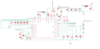
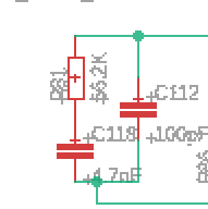
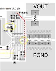
Can you please review our schematic and PCB layout and provide feedback on any improvements to enhance short circuit protection and reduce EMI? For reference, please ignore the lack of a shunt resistor, as we know it needs to be added.
We are also wondering why the TPS55288's built-in hiccup mode did not prevent damage during the short circuit.
Also, since we need to monitor the current drawn from the buck converter using our microcontroller, we plan to use a current sense amplifier to read the voltage drop across the shunt resistor. Is there a better approach for current sensing in this scenario?
Hi Hamid,
Thank you for reaching out. What is input voltage range, output voltage range, output current?
Can you provide the inductor current, SW1, SW2, Vout waveforms when short circuit occurs. I want to check the converter working condition. How do you conduct the short test?
About schematic, I think it is not clear enough.
1.Can you provide part number of MOSFET?
2.Recommend to add RC snubber in SW1 and SW2. It is not for short protection. It is for EMI performance.
3.What is rated voltage of VCC cap?
4.Compensation parameters are not clear to me. Can you provide the value? Also, please provide part number or datasheet of output capacitors for loop optimization.
About layout, please see my comments:TPS55288 layout reiview 20240903.pptx
Regards,
Mulin
Thanks Mulin,
Regarding waveforms, unfortunately, I can't provide the waveforms at the moment as we only have one board currently operational. We need it for ongoing testing, and performing this test might risk damaging the board.
1. MOSFET Part Number: The MOSFETs used are the same as in the EVM: IPZ40N04S5L4R8ATMA1.
2. RC Snubber for SW1 and SW2: Understood. Are there any recommended values for snubber?
3. Rated Voltage of VCC Capacitor: If you are referring to the capacitor connected to the VCC pin, it is rated at 16V. Other input and output capacitors are rated at 50V.
4. Compensation Parameters: The compensation network values are (same as in EVM): R: 56.2kΩ C (series): 4.7nF C (parallel): 100pF
5. Output Capacitor: Could you clarify which output capacitor you are referring to? If you mean capacitors connected to Vout they are as follow
1uF GRT188R61H105KE13D
10uF CGA5L1X7R1H106K160AC
220uF EEH-ZS1H221P
Regards,
Hamid
Hi Hamid,
Do you have current probe? I think it will be helpful if we can have inductor current waveforms. I think it is very safe.
What is input voltage range, output voltage range, output current? Need this for loop calculation.
RC snubber: 2.2ohm(1206)+2.2nF.
Regards,
Mulin
Hi Mulin,
No unfortunately I don't have a current probe.
This is a PD charger. The input is 24v and output is variable and can be between 3.5v to 20v.
Since this is a charger, the specific load connected to it is unknown, but the maximum current will be 5A.
Hi Hamid,
There is high possibility that your current compensation is not suitable and loop is not stable. Please try this compensation parameters: 15k+15nF parallel to 100pF.
Please follow my advice above. If you have more boards, please see SW1 SW2 waveforms to see if loop is stable.
Regards,
Mulin
Thanks, Mulin. We will adjust the compensation to the recommended values. Could this change address the issue of the buck converter MOSFETs being damaged due to a short circuit? Would it be safe to conduct a short circuit test after updating the compensation network?
Also, is a shunt necessary for short circuit protection, or is it primarily for voltage drop compensation? i.e. would it be safe not to have the shunt?
Hi Hamid,
I am not a hundred percent sure because I don't know the inductor current waveform. But I think this compensation will help a lot.
Which shunt do you mean? Can you help mark it in the schematic?
Regards,
Mulin
The shunt that measures the output current in the EVM and is in series with output and connected between the ISP and ISN pins. This shunt is not currently included in our schematic, but we plan to add it. We are curious whether the buck converter can handle short circuits without this shunt resistor.
Also, if we add the shunt on the output, should we connect it to the ISP and ISN pins using small resistors? I’ve seen recommendations suggesting a capacitor between ISP and ISN, along with small resistors connecting these pins to the shunt. Should we implement this, and if so, what resistor and capacitor values would be best to use?
Regarding the compensation network suggestions, most of the components, including the input and output capacitors, in our design are the same as those in the EVM. Could you explain why your recommended compensation network differs from the one in the EVM? What factors led to the different values for our board?
Hi Hamid,
TPS55288 can handle short protection without this shunt. It will be good that you add this function. Add 10ohm resistor and 100nF capacitor for filter is enough.
About the compensation parameters, because working input voltage, output voltage, output current are not same. Compensation parameters in EVM can not support all working condition even you do test in the EVM board.
Regards,
Mulin
Thanks, Mulin.
I have another question. There seems to be some conflicting recommendations between the datasheet, layout guidelines, and the evaluation module regarding how AGND and PGND should be connected.
The datasheet states, "AGND plane connects to PGND plane at the terminal of the capacitor at the VCC pin," but the layout guide shows pins 9 and 10 should be connected together. Could you clarify which approach is correct?
Image from datasheet.
Image from layout guideline.
Hi Hamid,
Sorry for confusing. Because these documents are updated all the time and some figures are not updated in time. "AGND plane connects to PGND plane at the terminal of the capacitor at the VCC pin," Please refer to this. Any problem please let me know.
Regards,
Mulin
Hi Hamid,
Please send friendship request to me and I will send you AD file.
Regards,
Mulin