This thread has been locked.

If you have a related question, please click the "Ask a related question" button in the top right corner. The newly created question will be automatically linked to this question.

TPS55288: Short Circuit Failure between VOUT and GND

Part Number: TPS55288

Hi,

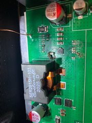
I have a TPS55288 based DCDC board. I have had two units fail with a short circuit between VOUT and GND, when operating at an input voltage of 10-15 Volts, an output of 13.5 Volts at a current limit of approximately 5 Amps. This should be well within the specifications of the TPS55288. Both units had been operating without failure for 2-3 hours, before the internal short occurred. Any ideas what may be causing this failure?

Other threads I have seen have always seemed to point towards layout issues, but I believe my design follows the guidelines from https://www.ti.com/lit/an/slvaer0b/slvaer0b.pdf fairly well.

See screenshot of schematic and layout below:


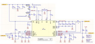
The board is a 4 Layer stackup, with the internal layers being solid ground pours underneath the entire area

  • Hi Cooper,

    I'll take a look at the schematic and layout and let you know the feedback as soon as possible. 

  • Hi Zac,

    To add some more info for you. I have scoped the SW2 pin of the TPS55288 and got the following plots:

    To me it appears that the ringing on the edge transients are excessive, with the voltage going negative to -1.4V (SW2 only rated to -0.3V). I also believe there is potential for the ringing on the rising edge to exceed the 25V limit on the SW2 pin.

    Do you think this would cause a failure like what I am seeing?

    If so, do you think this ringing is due to a layout issue? Or does our application need a snubber to help dampen this overshoot?

    I have been experimenting today and have successfully dampened the overshoot, but I would like to be sure this is our only issue before sending a new board design out for fab.

    Thanks for your help!

  • Hi Cooper,

    Below are my comments on the schematic:

    1. 100ohm resistance is too big for MOSFET driver R52, R53. It may cause unexpected problems. Suggest use 1ohm first.

    2. Add a 100nF ceramic capacitor across ISP, ISN pins to filter some noise. This helps to increase the average output current limit accuracy.

    For the layout:

    1. Add a 1uF ceramic cap and put it close to VIN pin as decoupling cap.

    2. It's necessary to put a 1uF or 100nF 0603 or 0402 package ceramic capacitor close to VOUT pin and GND pin (pin 11 and pin9). Currently the C13 is too far away from IC and may cause problems. Add some Vout vias and GND vias close to the pin 11 and pin 9.

    You can add one 1uF 0402 package ceramic capacitor on your current PCB and have a test again.

    3. Add 3-4 GND vias close to VCC cap C17. 

    4. Add 3 GND vias near pin 24. (like Vout vias near pin 26.) So that VCC gnd, analog signal components has shorter GND return trace.

    For more details, please read the TPS55288 layout guideline app note.www.ti.com/.../slvaer0b.pdf

  • Hi Zack,

    Thanks for these. I will roll these into the next revision.

    For an update on the ringing, with the 1uF capacitor installed on the current PCB there wasn't much improvement on the overshoot:

    Based on this, it looks like the RC snubber is needed. Below is a capture of the SW2 node with the snubber installed:

    The TPS55288 has now been operating for some time with the RC snubber installed and has not failed like the previous two, so do you think this looks ok?

    Thanks,

    Cooper

  • Hi Cooper,

    Thanks for the update. Did you put the 1uF close to IC enough? It helps to reduce the SW2 ringing. Yes, the RC snubber will help further improve the SW2 ringing. 

    You can share the layout next time. Thanks.

  • Hi Zac,

    We are still having a similar issue with the TPS55288 failing short between VOUT and GND. This is on the PCB I sent originally, with a 0603 1uF capacitor soldered directly to the VOUT and GND pins of the IC package, an additional 1uF capacitor between VIN and GND, and the inclusion of a snubber circuit. See picture below of the modified PCB:


    Our use case of the device is as a battery charger for a 4 Cell LiFePO4 pack (we are essentially implementing a two stage charge, first Constant Current and then Constant Voltage achieved by appropriate register setting via the MCU), so there is typically a battery powering VOUT whilst an input to the TPS55288 is not present. The input is a supply in the range of 10 - 15 Volts. Is there any issues with this? Looking through the datasheet I have not found anything to suggest our use case is unreasonable for this device, but the failures appear to always occur when an input is either connected or disconnected.

    We are reluctant to continue using this device due to these failures, unless we can fully understand what is causing these issues and rectify the problem. To us, it appears the remaining comments should result in a performance improvement, but do not likely contribute to the failures we are seeing.

    Thanks for your help

  • Hi Cooper,

    Per you description, this device should work for your application.

    I have two questions:

    1. Could you tell me what is U3 next to the output current sense resistor?

    2. Is the PCB a two layer PCB or four layer PCB?

    I still suspect the root cause is related to layout. The GND vias are far away from the VCC cap GND and IC GND pin (26 and 9). The big PCB parasitic inductance between VCC cap GND pad and IC GND will bring noise to IC internal logic circuit and cause wrong behaviors.

  • Responses for your questions:

    1. U3 is a current shunt amplifier. This is just so the MCU can monitor the output current. The inputs connected to ISP and ISN are very high impedance so should be having minimal effect on the signals heading back to the TPS55288.

    2. It’s a 4 Layer PCB. Internal Layers are continuous ground planes. The bottom layer is mostly identical to the top layer.

    Thanks for your help so far

    EDIT: I have put the oscilloscope on VCC and noise with an amplitude up to 0.5V is present in sync with each switching cycle. This is mirrored on the GND pad of the VCC cap but is not present on the GND of the output capacitors. So I would agree that the large parasitic inductance is having an effect.

  • Hi Cooper,

    Thanks for the update.

    1. Please note ISP, ISN pin is used for TPS5288 output current sense circuit, if the external MCU suddenly draw too much current from ISP, ISN or affect the ISP, ISN signal, it may affect the TPS55288 normal regulation.

    2. Got it.

    I would suggest update the layout and send me for review next time.