This thread has been locked.
If you have a related question, please click the "Ask a related question" button in the top right corner. The newly created question will be automatically linked to this question.
Tool/software:
Hello,
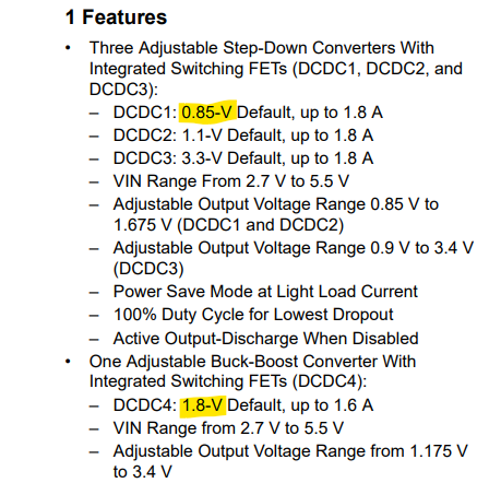
I designed a circuit using this PMIC to power an AM3352BZCZ30 solution along with the DDR3L and eMMC necessary for normal use.
After testing the circuit I can't power on the PMIC - at this point I have no FW on the AM3352 so the PWR_EN is pulled up, but from what I saw on the datasheet state machine (Figure 8-34) that shouldn't be necessary.
I'm betting on some detail that I must be missing from the design. I followed the advice from the datasheet and grounded the AC pin (the application of the board should power the PMIC immediately the moment external power is connected to it). I figured it may be due to having a floating PB pin and put a 100k pull up on it but it didn't solve the issue.
I'm re-reading the datasheet trying to find something that may be out of place, but can't seem to find the issue so far. Can you give me some help?
Bellow I attached the schematic I have implemented, to get your opinion. Thank you in advance.
Hi Ruben,
Like you mentioned, I noticed that the PB_IN pin is floating. If you are not using a push button in your design, please connect this pin to IN_BIAS (SYS5V) via the 100k pullup.
Are you able to capture any waveforms at all of SYS5V, PWR_EN, nWAKEUP, and one of the outputs? Just so I can maybe get a better idea of what could be happening here.
Best Regards,
Sarah
Thank you for the reply!
I have found that not all outputs are at a low voltage value, only two of them (V_CORE and V_3V3, in boldface on the table bellow) are still to reach their full output (coincidently all tests I did after the PB pull up only measured these two, so I didn't catch that the others were good…)
Name |
Nom Volt |
Test Point |
Measured |
V_DDR |
1.35 V |
C38 |
1.38 |
V_MPU |
1.1 V |
C40 |
1.14 |
V_CORE |
1.1 V |
C41 |
0.89 |
V_3V3A |
3.3 V |
C26 |
1.777 |
V_1V8 |
1.8 V |
C27 |
1.8 |
VRTC |
1.8 V |
C39 |
1.8 |
VDDS_DDR |
1.35 V |
C167 |
1.38 |
Here are the measurements you asked for (in all of them A is SYS5V):
B is V_CORE
B is V_3V3
B is nWAKEUP, the first image is at powerup and the second is during steady state.
B is PWR_EN, the first image is at powerup and the second is during steady state.
I found that PWR_EN and nWAKEUP didn't change state even after about a minute of measuring.
Hi Ruben,
Thank you for sharing the output values and waveforms! I notice that these values for V_CORE (VDCDC1) and V_3V3A (VDCDC4) are aligned with the default voltage settings for the TPS6521825.
I think these values may get confused with some of the TPS65218D0, which is an equivalent PMIC part, but it has different default output voltage values.
Are you using I2C in your system at all? You may need to write to the control registers to change these output values.
Best Regards,
Sarah
Thank you for the help, this is indeed the problem, I got confused with the similarities and ended up choosing the one with the wrong default voltage values...
It doesn't help that some images and tables of the datasheet indicate a different default value from the intro page:
I'll get to correcting things on my side and validating the circuit with the correct component, thank you very much for your help!
Hi Ruben,
I agree, some of the figures are misleading. I am looking into potentially getting this datasheet updated so we may avoid any future confusion.
Glad we found the issue, and glad to be of help!
Best Regards,
Sarah