This thread has been locked.

If you have a related question, please click the "Ask a related question" button in the top right corner. The newly created question will be automatically linked to this question.

UCC14240-Q1: No Output

Part Number: UCC14240-Q1
Other Parts Discussed in Thread: UCC14241-Q1,

Tool/software:

Hi,

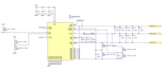
We have a UCC14240 connected to a UCC5870 Gate Driver as part of an inverter design. The output from the UCC14240 is 0.0V on all outputs, the device uses about 1mA at 24V.

Our required output is +20V, -5V. As such we have followed the UCC1424x design spreadsheet and have both FBVEE resistors at 49.9K, FBVCC resistors at 10K and 69.8K. ILim is 270R.

VEE-COM Capacitors are about 40uF, COM-VCC Capacitors are about 22uF.

Our VIn is +24VDC, the ENA pin is at 4.1V and the PG pin has a 10K pullup to 3.3V

Our schematic is below.

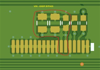
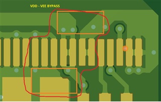
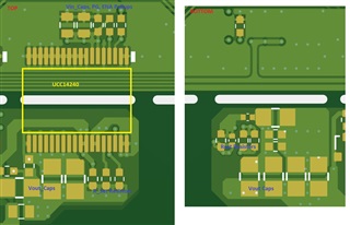
Our board layout showing the key compoennts:

Can anyone suggest what to check to determine why we are getting no output? We are totally lost as to why the devices have 0V output.

Thanks

  • Here are some recommended debug steps:

    1. For new designs, change UCC14240-Q1 to UCC14241-Q1. UCC14241-Q1 has some startup and noise immunity improvements that were not captured in UCC14240.
    2. Please follow the PCB design guidelines detailed in section 12.5 of the UCC14241 data sheet.
      1. The bypass capacitors should be as close to the IUC pins as possible. As with any high-frequency bypass capacitor, you don't want to place vias between the bypass cap and the pin you are trying to bypass. The goal is to force the current through the pass cap as best as possible.
      2. You could try and recover your PCB layout by placing 0402 size ceramic bypass capacitors direct across the VINP-GNDP and VDD-VEE pins. The 0402 size cap can be soldered right onto the UCC14241 package/pins - you can't get any better bypass then this...until your next PCB revision.
      3. The UCC14241-Q1 has an integrated, high-frequency transformer. You would not route signals under a transformer in a traditional power converter design and so it is recommended not to route beneath the UCC14241-Q1.
    3. Use RLIM configured as RDR arrangement shown in the Excel Design Calculator Tool.
      1. Your capacitor ratio is 1.81 but your output voltage ratio is 4. These should be matching as close as possible (minus any additional bias that might be applied to VDD or VEE). Are you sure you are applying the correct output capacitor ratio according to the recommended values coming from the spreadsheet?

    Steve

  • Hi Steven,

    Thanks for taking the time to respond.

    1. I have ordered some UCC14241's to try.

    2a.  Within reason our bypass caps are close, but maybe there is something about this device that makes it extra sensitive.  We've had similar issues with TPS55165 where we needed a bypass capacitor directly at the feedback pin 16. Having the cap even 1mm away from the pin caused device instability.

    Having said that, below is our input bypassing.

    And below is our VDD-VEE bypassing, with the exception that our bypass caps are on the rear of the board.

    2c. Noted thanks.

    3. We will mod the hardware to use the RDR configuration and we'll review the capacitor ratio. We did largely copy the UCC14241EVM-052 schematic and felt that this should have been a good starting point.

    We'll make the changes and report back, thanks for your help thus far.

    Cheers.

  • Hi Steven,

    We ended up with about 60uF between COM and VEE to get the device to startup.

    Final values for a +20,-5 System were:

    Cout1B = 20.1uF (12.4uF Spreadsheet Recommended)

    Cout2 = 10.2uF (3.2uF Spreadsheet Recommended)

    Cout3 = 60uF. (41.7uF Spreadsheet Recommended).

    The extra 20uF on Cout3 was the key.

    Thanks

    Stomp!