LM5143A-Q1: Abnormal Phase 3 Temperature Rise in LM5143A-Q1 4-Phase Buck at Vin = 50 V (No Load)

Part Number: LM5143A-Q1

Tool/software:

Using the 4-phase synchronous buck configuration,

Please find the schematic and quickstart design below.

7127.BUCK CONVERTER.pdf

LM5143A-Q1 Quickstart Design.pdf

we observed the following:

  • At Vin = 25 V, Vout = 15 V, the output current can reach 70 A.
  • At Vin = 40 V, Vout = 15 V, we are able to test up to 60 A, but at 70 Athe overcurrent protection is triggered and the output voltage cannot be maintained.
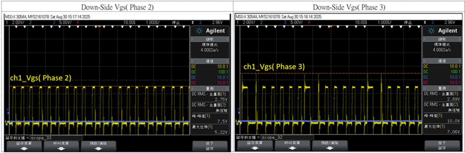
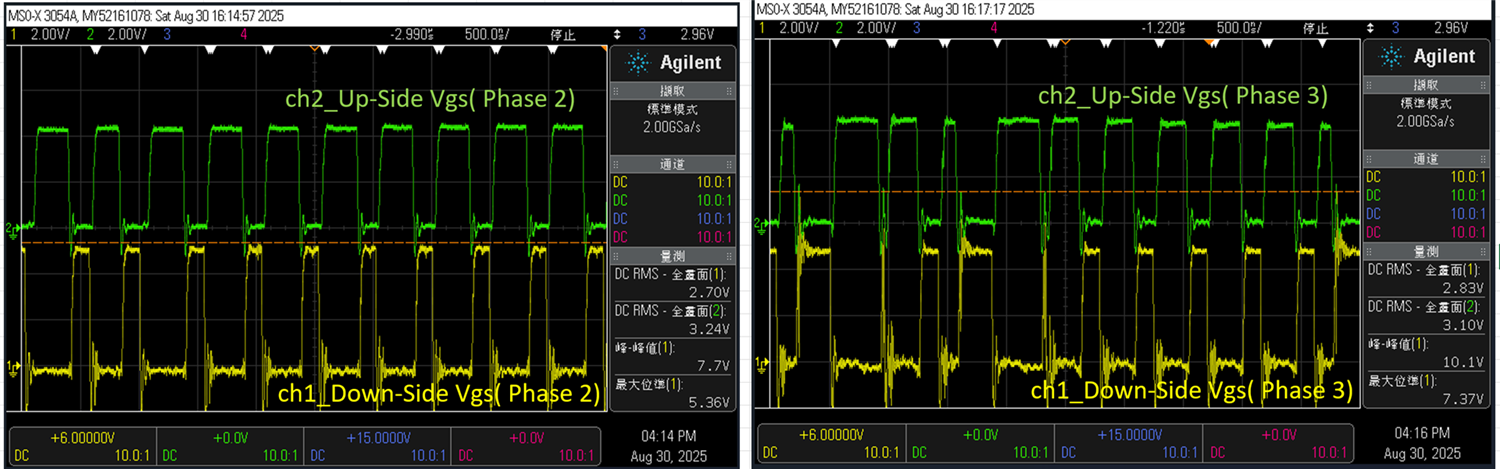
  • At Vin = 50 V and Vout = 15 V with no load, we observed an abnormal temperature rise on Phase 3 exceeding 100 °C. We measured the Vgs of the Phase 3 down-side MOSFET as shown in the figure below. For comparison, the Vgs of the Phase 2 down-side MOSFET shows a normal duty variation, while the Vgs of the Phase 3 down-side MOSFET exhibits abnormal duty behavior. We are not sure why this variation occurs. Or are there other possible causes?

Could you please advise how we can improve this?

Best regards,

YUMING


  • Hi Onkar:

    Thank you for your reply. We have identified the root cause of the issue, but we still need further clarification.

    We are implementing a 4-phase synchronous buck architecture using two LM5143A-Q1 controllers. Based on the datasheet SNVSCC1:

    • Page 6 indicates that connecting the primary IC’s DEMB pin to AGND enables diode emulation mode (DEM).
    • Page 31 suggests that the secondary IC should be configured with Mode = VDDA, FB1 = AGND, and FB2 = VDDA in order to enter DEM mode.

    In our current design:

    • The primary IC is configured with DEMB connected to AGND.
    • The secondary IC is configured with Mode = VDDA, FB1 = VDDA, FB2 = VDDA.

    During testing, we observed the following behavior:

    • With Vin = 50 V and no load, Phase 3 shows a high-temperature condition when the secondary IC is configured as Mode = VDDA, FB1 = VDDA, FB2 = VDDA.
    • When we configure the secondary IC as Mode = VDDA, FB1 = AGND, FB2 = VDDA, all four phases enter DEM mode at no load, and Phase 3 no longer exhibits the high-temperature issue.

    This raises two questions:

    1. Does configuring the two ICs differently for DEM operation cause this phenomenon?
    2. Or is this behavior already explained somewhere in the datasheet (SNVSCC1), and we may have overlooked it?

    We would greatly appreciate your guidance on the correct DEM configuration for a 4-phase implementation.

    Regards

    YUMING

  • Hello Yuming,

    The primary controller’s DEMB pin determines whether it operates in DEM (Discontinuous Conduction Mode) or FPWM (Fixed-Frequency Pulse-Width Modulation). The secondary controller uses the FB1 pin to select its operating mode.

    In your configuration, FB1 is connected to VDDA, forcing the secondary controller to operate in FPWM mode. This results in higher losses in phase 3 compared to the other phases.

    I would suggest operating both controllers either in DEM or FPWM 

    Thank you

    Regards

    Onkar Bhakare

  • Hi Onkar:

    Thank you very much for your valuable suggestions. We believe the issue has been clarified, and this topic can now be closed.

    Thanks again for your support.

    Regards

    YUMING