This thread has been locked.

If you have a related question, please click the "Ask a related question" button in the top right corner. The newly created question will be automatically linked to this question.

TPS79650 and TPS71733 Lock-Up

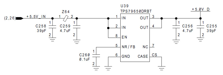
We are using two LDO's in our design: TPS79650 and TPS71733.  When testing at temperature of +70C ambient (with approximately 10-15C internal temp rise) we are seeing these devices lock-up while power-cycling.  Symptom is reference appears to go to 0.8V instead of 1.2V as monitored on the noise reduction pin.

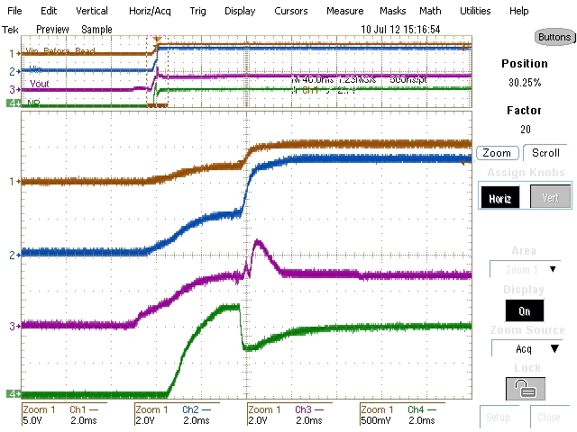
The block diagrams of the TPS71733 datasheet show a selection circuit between a high and low reference voltage based on a Vout of 1.6V.  The TPS79650 block diagram does not show this circuit but it appears it also has this function based on the failure effects.  Can TI please provide details on this function and how the decision between the two references is made?  This would include timing of the decision and inputs.  I would like to know if further reduction or removal of the noise reduction capacitor can help address this issue by speeding up start-up time.

  • Hi Shawn,

    Can you attach a circuit schematic of how the LDOs are being used? Also, waveforms (VIN VOUT EN) showing what the problem might be would be helpful (I am unsure what you mean by lockout).

    Regards,

    Darwin

  • Hi Darwin,

    Thank you for the response.  Basic schematic is below.  It is being used to power several digital gates and three general purpose low-speed ADC's.  Normal operation is 5V at the output with ~1.25V at the NR pin.  Failure condition is 0.8V at the NR pin and ~3.2 V at the output (0.8/1.25 * 5).  Failure can be induced by power cylcing the unit multiple times at temperature.  It will stay locked up even when bringing the unit back to room temperature and requires a power cycle to return to normal operation. Reducing the NR cap to 0.01uF helped some units but not all.  I'll work on instrumenting the unit to capture waveforms.

    Shawn

  • I'm working with a local TI support engineer but I thought I would post waveforms in case someone had a similar issue.  The LDO powers circuitry that uses both 5V and 3.3V rails.  The 3.3V turns on approximately 5 ms before the 5.5 V input to the LDO, and the ragged Vin voltage appears to be backfeed from the other supply.  We are investigating whether this contributes to the problem.

    1. Trace 1 - +5.5V_IN
    2. Trace 2 - TPS79650 IN/EN Pins
    3. Trace 3 - TPS79650 OUT Pins
    4. Trace 4 - TPS79650 NR Pin

    Normal Startup

    Lock-Up

  • Second image was lost in original Post.

    Lock-Up

  • Hi Shawn,

    The second waveform does seem unusual. Would you be able to measure the input current and output current under this condition? Also, it may help to increase the input capacitor so that the VIN signal does not stair step as much.

    If this does not improve performance, it may good to test only the LDO by removing the input filter, load, and using a power supply at the input of the LDO to see if the same fault occurs. 

    Regards,

    Darwin

  • Hi Shawn,

    I am also working with "the other" Shawn from TI on apparently this same problem.   The "wobbley" startup is typical of the very fast startup circuit of this part.  When the output capacitance is being charged at such a fast rate the Iout=C*dVout / dt is often high enough to either hit current limit, or more likely, to pull down the Vin voltage. 

    The concern I have regarding your oscope plots is the fact that Vout rises with/before Vin - which could indicate that either the UVLO is not working or something else is causing the LDO to partially power.

    Regards

    Bill