


Hi Team,
Our customer are studying usage of TPS63010 at the following conditions.
Could you please let us know if you have any information and advice?
[Conditions]
Vin=2.1V to 4.2V
Vout=3.3V
Iout=0.5A (peak 1A)
--------------------------------
[Q1]
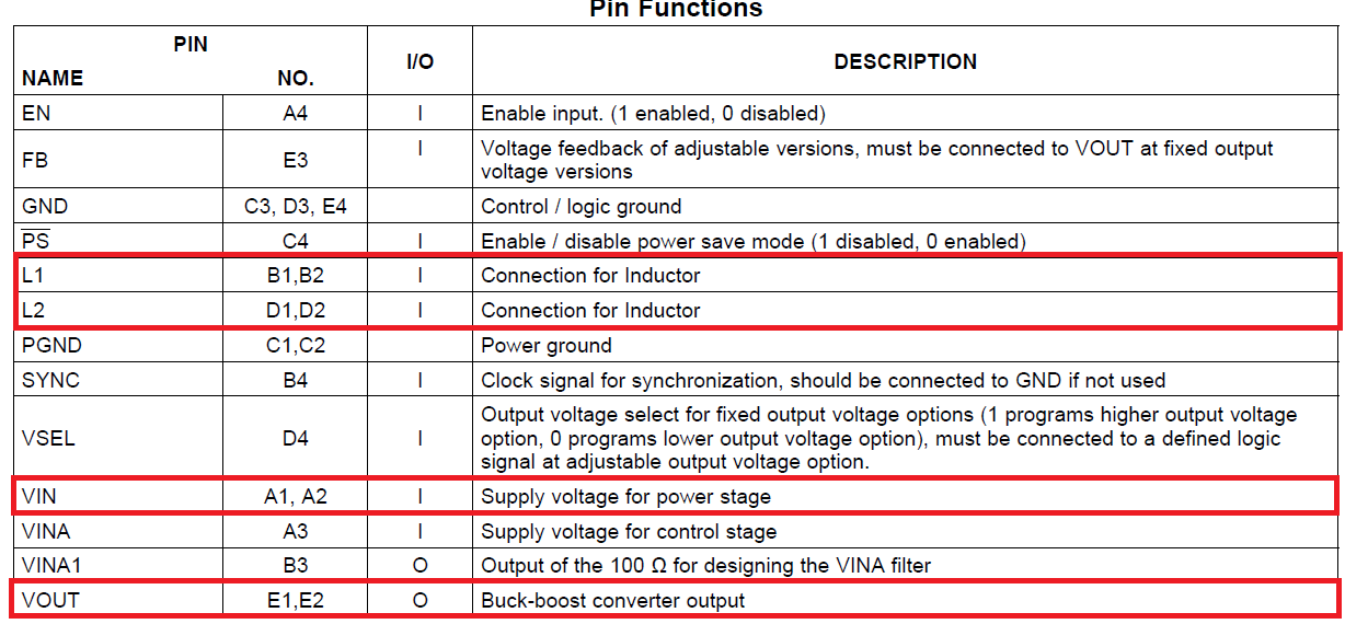
Why are “VIN”, “L1 & L2”,” VOUT” pin assigned the 2 pin?
I guess that this reason is to reduce the parasitic resistance of those pins.
Therefore, the power loss of this device is suppressed.
Is my understanding correct?
------
[Q2]
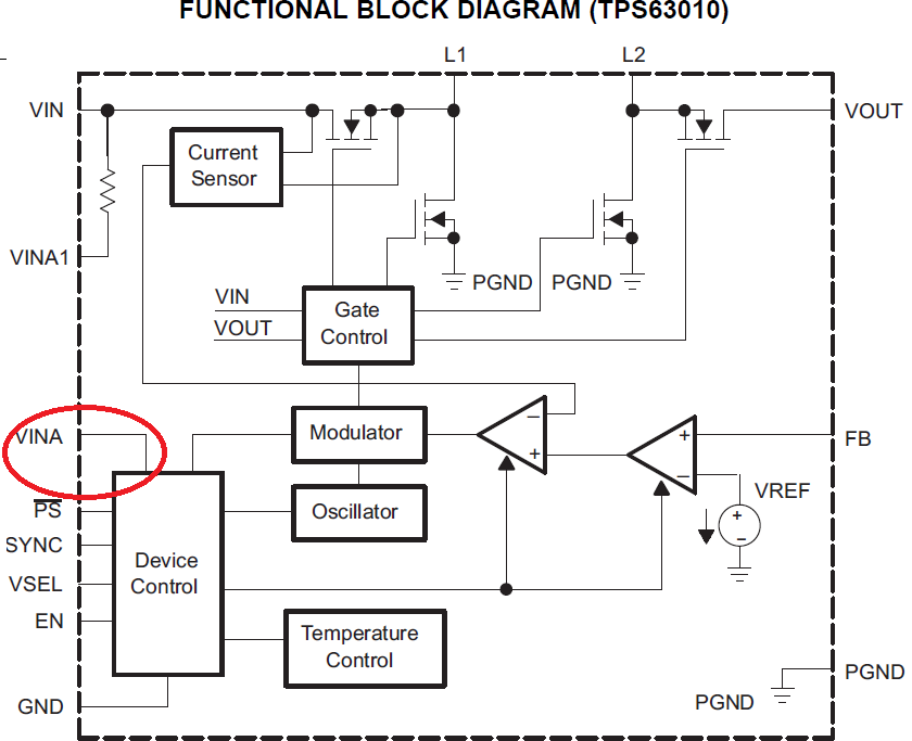
They would like to decrease the power loss of TPS63010(ADJ type).
I’m understanding that VSEL pin connect the internal control block.
To decrease the power loss, which do you think is better “VSEL=High(VIN)” or “VSEL=Low(GND)”?

------
[Q3]
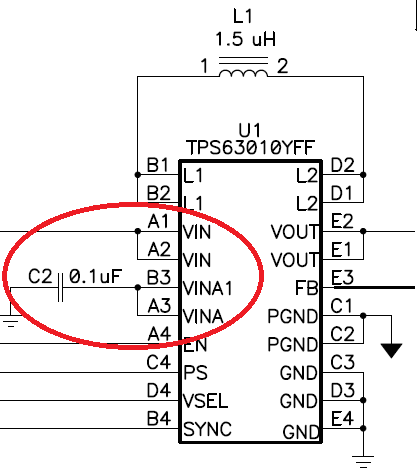
We would like to know the function of VINA1 pin.
According to datasheet, VINA1 pin is “Output of the 100 Ω for designing the VINA filter”.
So, I’m understanding that VIN is filtered for VINA by the internal 100Ω and C2=0.1uF.
Is my understanding correct?

And, is a connection method of EVM recommended?
--------------------------------
Regards,
Kanemaru

