This thread has been locked.

If you have a related question, please click the "Ask a related question" button in the top right corner. The newly created question will be automatically linked to this question.

Vgs and Vds signals for the leading leg (PS ZVS)

Other Parts Discussed in Thread: UCC28950

Hi,


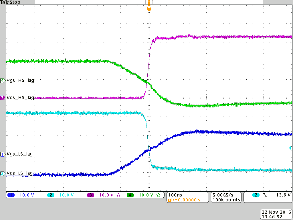
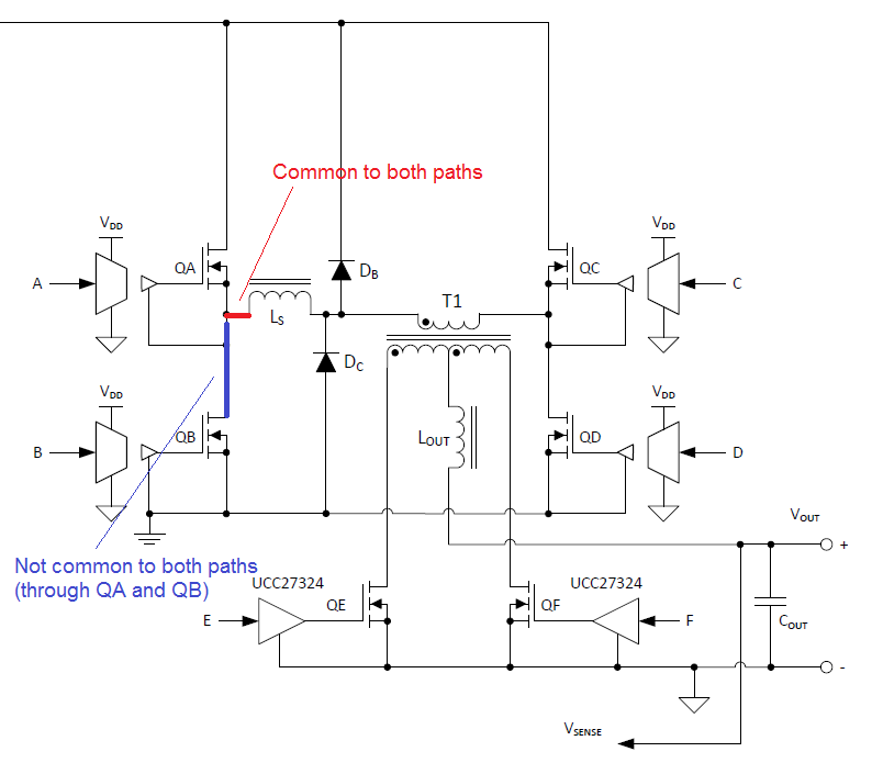
I posed this question in an earlier post, however now I have better plots and maybe someone could help me. I designed a PS ZVS converter and the leading leg has some ringing on Vds which is ousted for the lagging leg. Does anyone know due to what factors I got this behavior. Is it normal (Vds drops before Vgs rise)?  
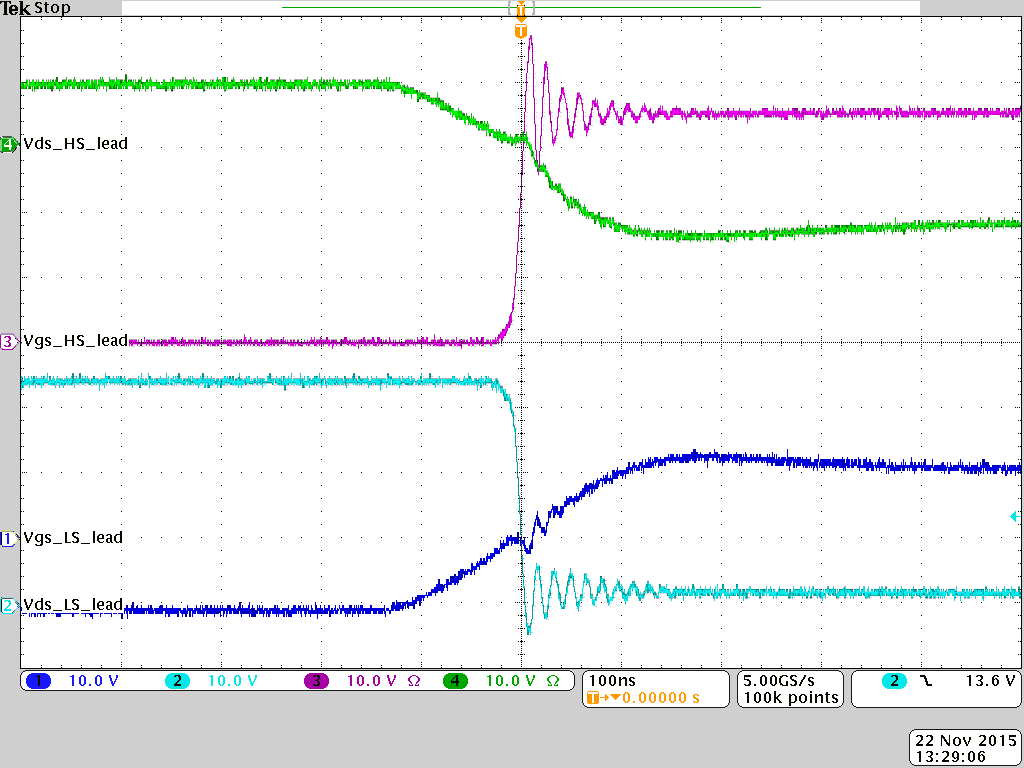
Currently the Tdelay is similar for the two legs but I believe this shall not affect the functionality.


I the previous post I have asked also about some oscillation due to compensation loop. It proved that the Rsum was to high and the current compensation was not effective (maybe it helps).

  • Hi Florin,

    Which TI controller are you using?

    Regards

    Peter
  • Hi Peter,

    The controller I am using is UCC28950.

    Thank you for your support!
  • Hi Peter,

    Sorry for disturbing you again, but can you help me with the above question?

    Thank you very much!
  • Hello  

    There are a couple of things I would check - First, do you have the diodes labelled DB and DC in Figure 48 of the UCC28950 datasheet. We changed the datasheet recently to RevC, please double check that this is the version you look at.

    I would also review the PCB layout for stray inductance in the MOSFET drain and source connections.

    Regards
    Colin

  • Hi Colin,

    Many thanks for your quick reply!

    Indeed I omitted DB and DC in my design, but adding these two would only clamp the oscillation to the rail I presume. I am very interested in the phenomenon generating these oscillations. As the stray inductance adds to the leakage one I am not very sure that the impact coming from this side is conclusive.

    I will add the diodes and re-check the behavior.

    Also, is interesting that the sluggish leg drain voltage is not oscillating:

    For sure there is an LC oscillation but I am not very sure why. If you could help me I would be grateful.

    Thank you,

    Florin!

  • I normally stick to the TI nomenclature and call the leading leg the AB leg and the lagging leg the CD leg - I do this mainly so I don't confuse myself so I'll explain it as follows. Basically, there is more energy in the system (mainly in the output inductor)when the AB leg turns off - this has two effects - first, it makes it much easier to achieve ZVS and secondly it increases the amplitude of any unclamped LC resonances. When the CD leg is turned off there is much less energy available to drive the ZVS transition. This transition will be slower as a result and the LC resonances will also be less energetic.

    It's difficult to explain it in text but currents generate a magnetic field and this field stores energy. If this current is in part of the circuit path that is not changed when the switches are turned off and on then it can continue to flow - eg any current in a PCB trace in series with the inductor (red above). Currents which exist in a PCB trace which is switched will generate a magnetic field which stores energy. When the switch is turned off, this current will continue to flow and the inductive energy is released generating voltage spikes. An example is highlighted in blue above.

    This is  why PCB layout is very important to a successful product.

    I hope this answers your question - feel free to re-post with any further queries.


    Regards
    Colin