This thread has been locked.

If you have a related question, please click the "Ask a related question" button in the top right corner. The newly created question will be automatically linked to this question.

BQ24610: HIGH SIDE FET TEMPERATURE

Part Number: BQ24610
Other Parts Discussed in Thread: CSD18504KCS,

Hello,

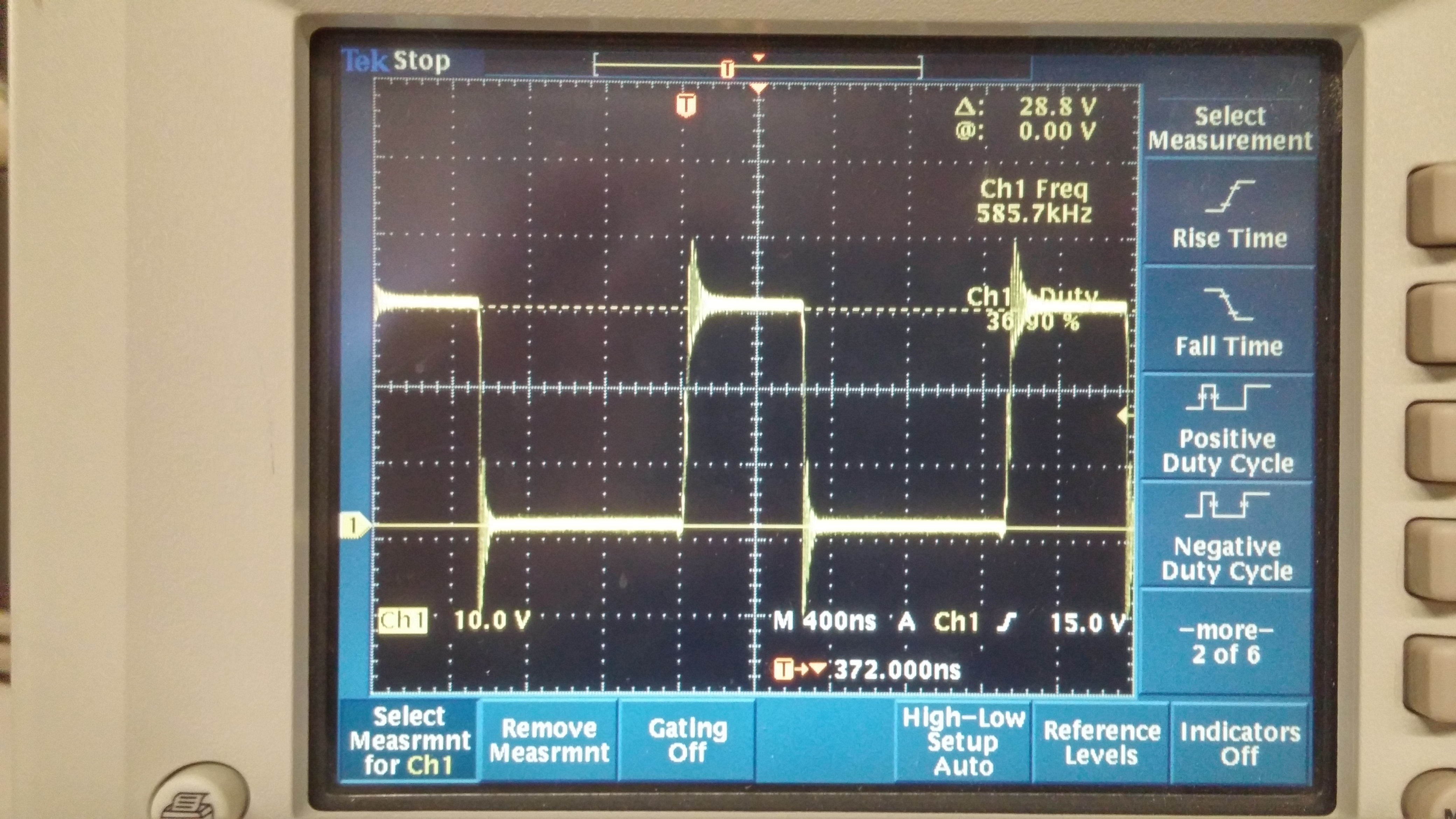
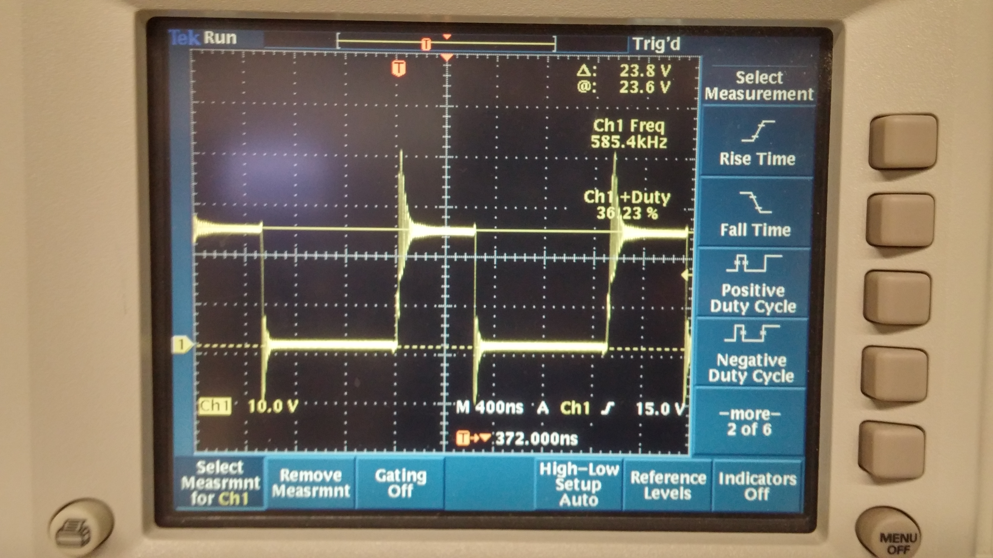
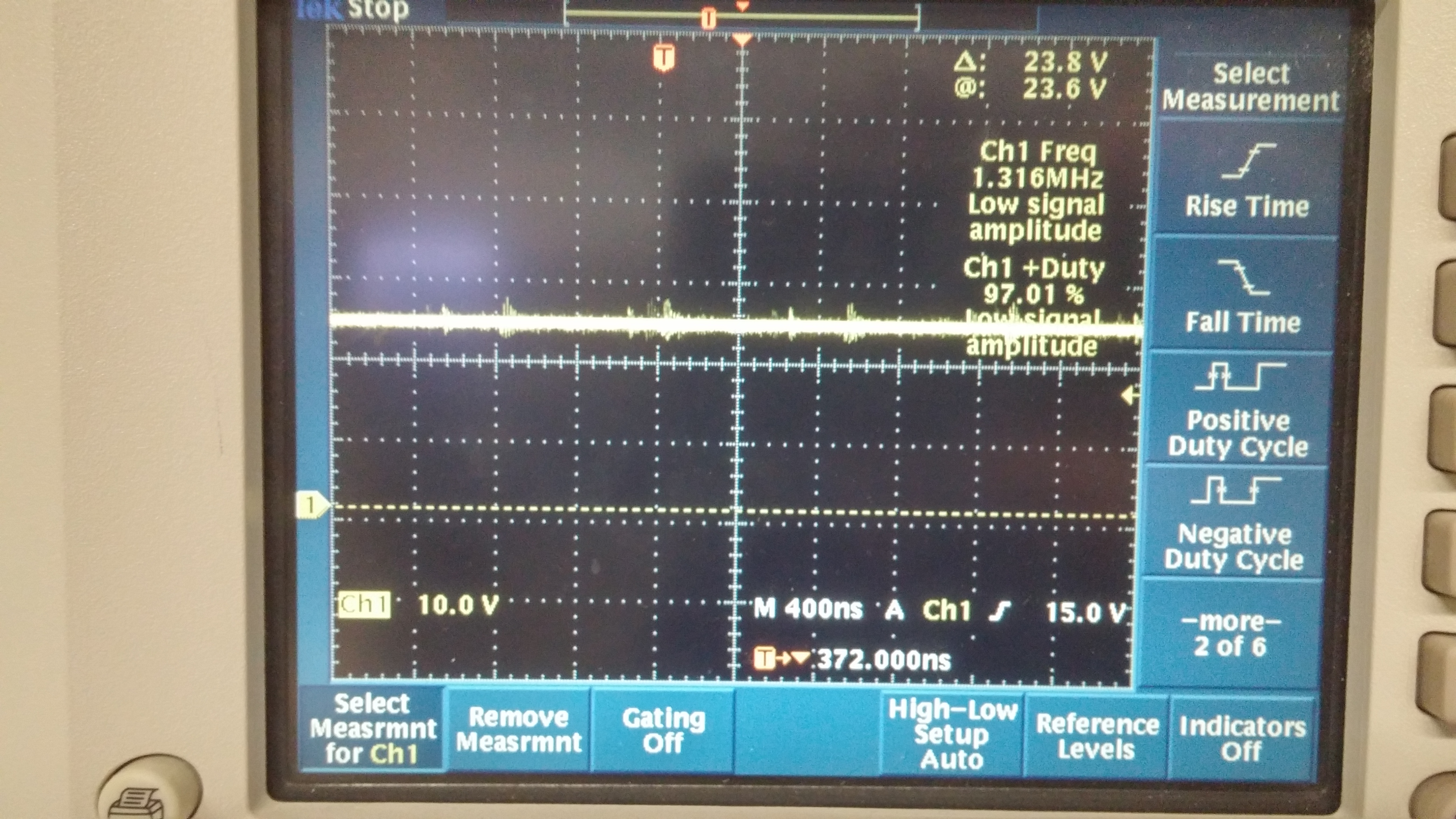
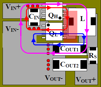
We are using a BQ24610 to charge out 8.4V 20Ah battery. We are using a 24V input supply as the power source and the battery charge current is 9A. We have had issues with very high temperature rises on the output fets attached to the Hi and Low side driver, particularly the high side. Over the 2 hours or so the battery is in  constant current mode the fets can rise as much as 100C or more from room temp. Current our fets are CSD18504KCS next fets with a 6225B-MTG heatsink attached to them. 

I did a little math for resistive and switching loses and I get something like 5W to 8W worst case however we measure a loss of around 14W to 16W for the battery charger. I guess I must be missing something and I was hoping you could point me in the right direction.

A copy of my schematic for this circuit is attached.SCHEMATIC1 _ 07 BATTERY CHARGER.pdf

Thanks,

John

  • Hi John,

    That certainly sounds weird. If the FET can handle up to 10A, which I know it does, then it should work as long as the heat is being dissipated properly.

    Either way, we recommend using surface mount FETs, as this would give a cleaner switching waveform and better response on the converters due to less parasitics and shorter routing.

    If you have a scope available to use, please probe the PH node, HIDRV, LODRV and VCC please. I want to see if there are any abnormalities in the switching waveforms.

    Regards,
    Steven
  • So, I have attached all the scope captures u wanted. 

    Thanks,

    John

  • Hi John,

    These scopes shots have a lot of ringing and could cause some problems. We need to mitigate these.

    1. The most easiest way to minimize is to add an RC snubber to the PH node.

    2. Add a series resistor to the HIDRV and LODRV traces to reduce dV/dT on the gate of each FET

    3. Improve the layout by optimizing the power stage of the converter using surface mount FETs. The COUT are very close after the sense resistor and the CIN are before very close to the QH drain.

    Did you ground the probes properly? Try to get the ground pin as close as possible to the test point on your board using a short cable to reduce any parasitic.

    Regards,

    Steven.