This thread has been locked.

If you have a related question, please click the "Ask a related question" button in the top right corner. The newly created question will be automatically linked to this question.

UC3842: Regulator not oscillating correctly

Part Number: UC3842
Other Parts Discussed in Thread: TL431

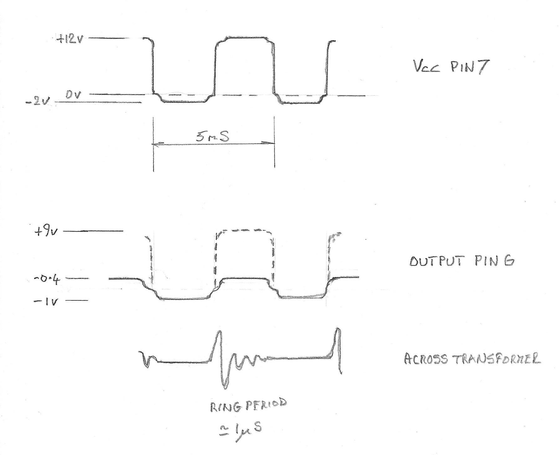
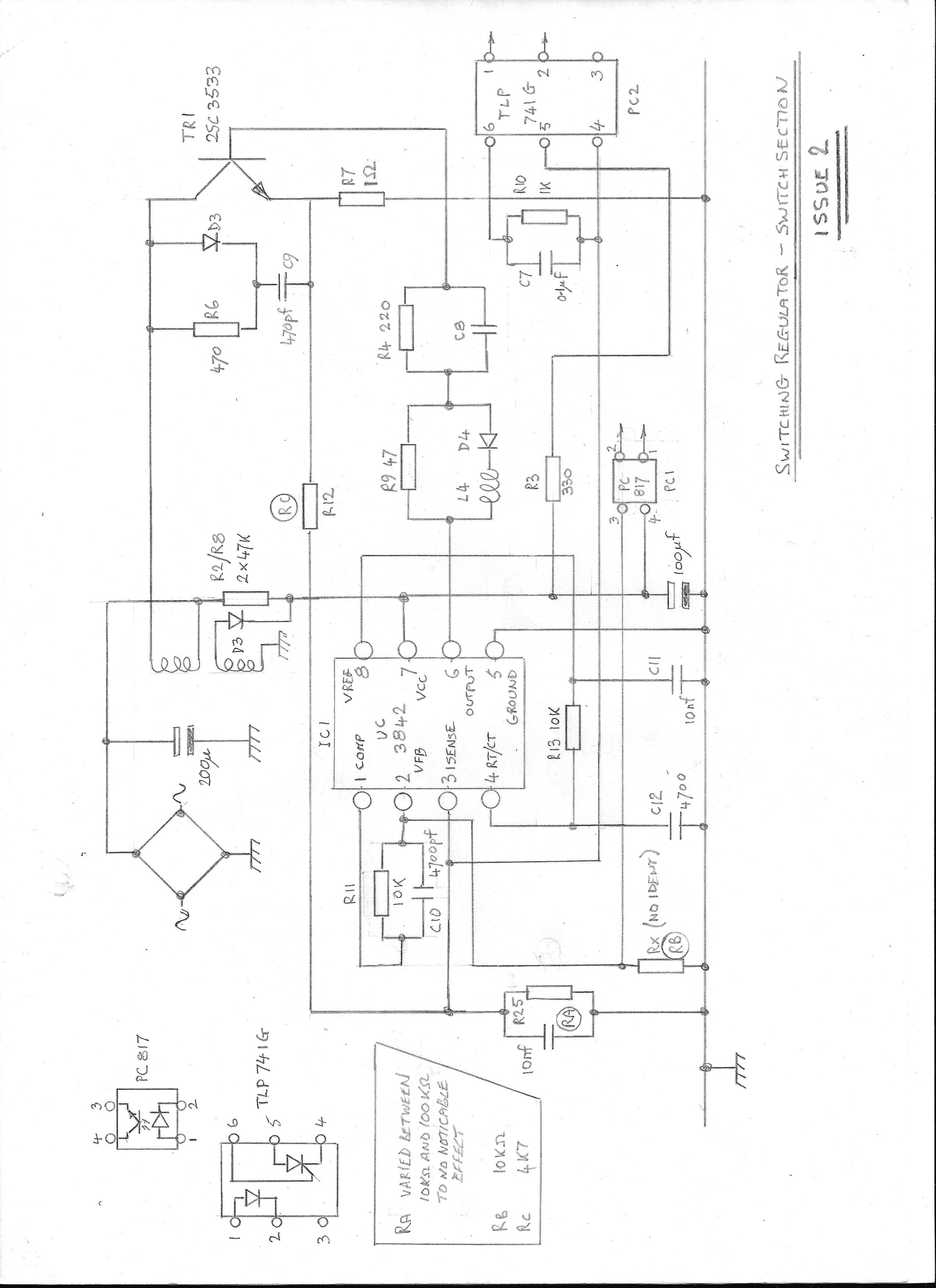
I am trying to repair a fairly ancient (probably 1970s) power supply from a Japanese (Mitutoyo) Digital Readout unit on a vertical mill.  The problem is restricted to the power supply.  Unfortunately three of the resistors on the board have burnt out and so their values are unreadable.  They were 1/8W - so not intended for high power - and I traced the cause to a mechanical problem causing a short.  Based on the data sheet I have tried numerous values but, whilst it is trying to oscillate, it is only 'hunting' and pulsing.  I have traced the circuit diagram for the switching section of the supply; the regulated outputs are derived from the secondary of the transformer (not shown in the diagram) and I do not think that part of the circuit is faulty.  The diode side of the two photocouplers connect to the regulated supplies.  The mystery resistors are labelled RA, RB, RC.  Any ideas?

Many thanks in anticipation!

  • John O.,

    Thanks for sending along your questions.

    Can you verify that the part is biased properly? The best way is to probe the Vcc to guarantee its above UVLO levels.

    What are you getting at the output pin? Can you provide waveforms for  that?

    It sounds initially like it's in UVLO or hitting a fault so let's try to rule those out first. But we need to talk through some waveforms to understand. It will be good to understand your input and output conditions while you are testing.

    Is it failing to startup or does this problem occur after startup at some other condition?

    Regards

    John

  • John S,

    Many thanks for the quick response. Just for background, although I am FIET and should have good overall knowledge of electronics, my career has been in microwave engineering so my experience in this area is a little sketchy!

    I will need to make a few specific measurements to answer your questions. I'll try to get these done today and get back to you.

    Many thanks,

    John
  • John O.,

    Sounds good. Thanks. Note that it's usually easier to "use rich formatting" to post images to e2e here. Note the link in the reply box. When you attach it will look like a big grey box gets loaded into the reply window. That's normal. Just keep posting below it no problem.

    Regards

    John S

  • John S,

    As a new user I'm rather confused by the posting images process. I have scanned the image as a jpg and inserted it in a Word document and saved it as an rtf.  The instruction above tells me to use copy/paste using the 'Paste from Word' button.  It seems to only work with text.  The link symbol you refer to in the toolbar is greyed out.  So, for now, I've inserted it as before.  Apologies.

    The waveforms are hand drawn but I hope they are near enough for you to have some idea of what is going on.  It does this every time from switch on and never operates correctly.  The waveform is synchronised with 50 Hz mains.  The values for RA, RB and RC that I have inserted are 10k, 1k and 4k7 respectively.  I am fairly confident that I have traced the circuit accurately but you may spot any obvious schematic errors.  At least it is only single sided/single layer!  The circuit has obviously worked for many years so there cannot be any fundamental changes.  All active devices have been either checked or replaced.

    Thanks,

    John O

  • John O.,

    sorry to hear the paste function was being difficult. waveform images from your scope with multiple signals is almost always the best way to debug with you.

    From what you've shown, if Vcc is going low(below UVLO off), the controller is shutting off constantly. In that way, I don't think it wold regulate the main output voltage. Is this what you expect? I would suggest adding more capacitance to Vcc so that the IC stays on. It should control the output on/off to create a regulated output but the Vcc should be above UVLO at all times.

    Regards,

    John S

  • I had wondered about that but on the basis that 100 mfd was originally fitted and must have worked I assumed that something else was at fault.  I removed the capacitor and checked it for value and leakage and it appeared to be OK.  However, I will try some additional capacitance to see if it stabilises Vcc.  Did you have any thoughts about the values for RA, RB and RC?  Incidentally, I have tried to get information from Mitutoyo but they refuse to help!

    Regards

    John O

  • I tried an extra 220mfd on Vcc and it did improve things.  Vcc is now stable at about 14V.  The oscillations are still only a series of rings (as previously described) but are now almost continuous to the point where there is actually some regulation taking place in the 'other half' of the circuit.  But the various DC outputs are not stable, so we are still looking for a stable oscillation in the switch.

    Regards,

    John O 

  • Hello John,

    I was asked to follow up on your issue while John S. is out of the office. While reviewing the original schematic you posted above, I noticed some unusual connections. I would ask you to re-examine the board closely and confirm that the circuit arrangement does follow your schematic or please make corrections. Items that I find unusual or ambiguous:

    1. The unknown resistor designated RA: is it located in the line between RB (Rx) and the R11-C10 network and simply not shown, or is RA = R25 to the left?
    2. If RA= R25, is R25 actually across the 10nF cap from pin 3 to GND, or should R25 be drawn in the line above RB?
    3. Should the line at RA go up to the COMP input, or should it go to the VFB input?
    4. Is the current sense resistor R7 value really 68 ohm? Or could it be 6.8 or 0.68 ohm?
    5. Does the output of PC2-pin4 truly go to the RT/CT pin of IC1, or does it really go elsewhere (such as IC1-3 ISENSE)?
    5. Is the RCD snubber network truly across TR1 from C to E, or does C9 go to the bulk voltage rail at the 200uF bulk cap?
    6. Are the 10k, 1k, 4k7 values for RA, RB, RC the actual original values of the burnt resistors or are they best guesses for test purposes?

    I ask about RA and R25, because as it is drawn now, the emitter of PC1 drives the IC1-1 COMP input directly, and there would be no reason to have the R11 and C10 components to VFB. Also, as drawn, R25 forms a divider with R12 (RC) so it would attenuate the current sense signal to ISENSE.
    R7 at 68R seems very high to me. With a 1-V limit at ISENSE, it would allow a peak current of only ~15mApk which would deliver very low power, even with a 230Vac input. But I could be wrong, because a divider to ISENSE would increase the peak and the output power. It just seems like a strange arrangement to me.
    PC2-pin4 output going to RT/CT is also strange. The latest UC3842 datasheet shows a similar shutdown circuit for external protection in Figure 20 on page 18. It is a different arrangement, but uses an SCR to pull up on ISENSE. Your drawing uses the opto-SCR to pull up on RT/CT, which doesn't make sense to me.

    I wonder why RC (R12) would burn out. If it were a high value passing signal-level currents, it should not overheat. However if R7 was damaged and failed open-circuit, then when TR1 was driven it could over load the ISENSE input, which might fail and then overload R12. That is speculation at this point, depending on the true value of R12. Presumably, if R7 opened, the emitter of TR1 could rise only as high as a Vbe-drop below the base drive voltage which is limited to VCC.

    The RT/CT values indicate it should be switching at ~36kHz (when it works).
    I suspect that there may be more damage to this supply than meets the eye. Whatever burnt the resistors may have also damaged the IC at the inputs where those resistors connect. I recommend to replace the IC.
    Also, the 50Hz waveform at VCC (pin 7) suggests that the input diode bridge may be damaged as well. I'd replace that, too. VCC should be DC voltage with very little ripple. Certainly not 12V to -2V with a 5ms period (which indicates 200Hz).
    And if something damaged the bridge, it could be that the main transistor TR1 is also blown out. Please check that. Faults that blow out several resistors rarely confine their damage to only the resistors.

    On the other hand, the odd VCC waveform may be the result of your probing method. If you have a Grounded oscilloscope and probe the non-isolated primary side of the supply, the signals will ride superimposed on the AC input.
    You MUST use an ISOLATED AC input (or apply an isolated DC input directly to the bulk voltage rail) and Ground the primary-side return path to properly view the primary-side signals.

    Can you please provide the normal input voltage for this supply, and estimate the total output power level?
    And please recheck the schematic connections; I suggest to use the example application of Figure 25 in the latest UC3842 datasheet (click on the link to download it) as a reference guide. (Some of the example circuits may not be used, of course. )

    Regards,
    Ulrich
  • Dear Ulrich,

    Wow - that's quite a response - many thanks.  I will need some time to digest your comments and to do the additional checks.

    I thought I had traced the circuit accurately but, like you, I was surprised at some of the connections when compared to Fig 25 on the data sheet which I downloaded at the start of the investigation.  I will go over it again very carefully.

    The burnout was caused by a short circuit to the case due to the failure of some insulation so I am sure it was not part of the initial failure.  I have replaced the IC, the two photocouplers and the transistor and I am confident that they are OK.  I have also checked many of the passives out of circuit, particularly the capacitors.

    I am making measurements with a dual channel oscilloscope set to CH1 + CH2 with CH2 inverted.  The mains input is isolated and, although I haven't shown it on the diagram, is via a balanced LC filter.

    I will get back to you with my findings but, once again, many thanks,

    John

  • Taking you points in turn:-

    I'm sorry for the confusion with the labeling: R25 is RA and is in parallel with the 10nF capacitor between ground and pin 3.
    The line at RA should, as you rightly say, go to pin 2 VFB.
    Similarly, PC2 pin 4 does go to pin 3 ISENSE.
    Both these errors were transcription error when I made a fair copy of my rough diagram!
    R7 is indeed 0.68 - my misreading of the value.
    The RCD snubber network really is as I have shown it - I have triple checked this.
    The values I have used for RA, RB, RC are my best guesses. The burnt-out resistors were unreadable so I have based their values on the data sheet.

    I have replaced all the active components. TR1 and R7 were damaged (R7 o/c), as was the UC3842. The diode bridge is fine - I checked it out of circuit with a meter and also tried another one which gave identical results.

    The nominal input voltage is 220V, 50Hz mains. I find it difficult to estimate the power output but I suspect it is not particularly high. The instrument is essentially measuring inputs from two remote sensors, carrying out some processing and displaying the results on LED displays. I imagine that the LEDs will be the biggest drain and the logic is probably Schottky TTL. I am reluctant to get into this side of eth equipment because it is in a separate sealed unit. One interesting point - not sure how relevant - is that one of the outputs has a 1 farad (yes, that's one farad!) capacitor across it. The most likely reason for such a massive value is that the inputs from the sensors are very small and there must be no chance of any ripple. Looks like overkill to me.

    I hope this clarifies things and maybe points to a solution. Sincere apologies for the errors. I would welcome any ideas about likely values for RA, RB and RC.

    Kind Regards,

    John
  • Hi John,

    Thanks for the clarifications and additional information. Because of the D3 auxiliary winding connection and the lack of slope compensation on ISENSE, I will assume that this is a DCM flyback design. The huge cap on one of the outputs essentially makes it look like a short circuit for a long time (relatively speaking) during power up. Since the UC3842 can go to nearly 100% duty-cycle, it may in fact go into CCM during start-up, but back in the '70's they may not have cared about sub-harmonic oscillation, or even been aware of it, as long as it started up okay. We'll have to assume the power level is likely to be somewhere between 20 and 100 W.
    The values you chose for RA, B & C seem to be reasonable guesses, based on the DS example schematic.

    Based on this I think we can start debugging the circuit. I recommend that you keep the supply unplugged and apply an external 12~20V dc source to the VCC node and GND. This way you can probe non-differentially with 2 channels. Slowly ramp up the VCC and monitor VREF and RT/CT. Once VCC reaches the 16-V turn-on level, VREF should jump to 5V and RTCT should show a sawtooth waveform at 30~40kHz (I calculate 36.6kHz). If neither of these happen, the chip needs to be replaced again. Dial down VCC to about 12V for the rest of debug.

    Also, I would disconnect R3 from VCC until later after control debug. It is a protection circuit for something on the secondary, but let's keep it out of the picture until we see that TR1 is driven properly.

    Assuming success so far, the OUTPUT pin 6 should be pulsing at 36kHz at nearly 100% duty. This is because the opto PC1 is off (no secondary power) so RB (1K) is pulling VFB down to GND and COMP should be pegged at ~6V. This generates the highest voltage at the PWM comparator and the lack of signal at ISENSE drives the PWM width to maximum.
    ISENSE may have some small pulses on it due to the base drive current through R7, but the 10nF cap can absorb much of that leaving mostly a vague offset voltage.
    Guessing RC = 4.7K is reasonable; but 10nF on ISENSE is pretty stiff, so they must have had to filter a lot of noise or suppress the turn-on spike or something. I am perplexed by RA across that cap. It divides the signal from R7, making it appear to be smaller in value. Since the internal max limit for ISENSE is 1V, the net effect is to allow a higher peak than 1V/0.68R = 1.47Apk. A very low value for RA would make this peak in the 10's or 100's of amps, so that is absurd. A very very high value would barely increase that peak. 10K effectively increases it by 1.5x which seems fairly high increase, unless they couldn't get a lower value for R7. My guess is that R25 (RA) may be an adjustment resistor to tweak the peak current to get the full power needed, whereas the next typical resistor 0.47R might have been too coarse of an adjustment. R25 might actually be somewhere between 33K and 100K, but that's just a guess as good as yours.
    47K increases the Ipk by 10% to 1.62Apk, for instance. I recommend to start with the 10K you have here and get the supply running. The loop will reduce Ipk to regulate (once it works), and you can increase the R25 value later until it doesn't provide enough power to regulate anymore, then back down again to give it some margin.

    The bulk rail may charge up a bit when the OUTPUT drive TR1 and the base-collector junction conducts into the bulk. It shouldn't go higher than a couple of volts. Once Vbulk is charged up, all of the base drive current should go through R7, which should show narrow spikes of about 0.15V due to the higher base current through the speed-up cap C8. After that the base current drops to ~41mA due to R4 limiting.

    I am also perplexed by the lack of a resistor between PC1 emitter and the VFB input (as seen in the DS Figure 25 as Rfbg). This means that any tiny change in emitter voltage is immediately amplified by the full gain of the internal error-amp, and it sounds like a stability nightmare. But I may be wrong if the impedance of the PC817 opto is high enough that the emitter voltage doesn't change much or quickly.

    If everything looks like it is working correctly and the TR1 base and emitter are toggling, you can apply a 2nd dc source to the bulk voltage rail and slow crank that up a few volts at a time and look for switching waveforms at the collector of TR1 and at the anode of auxiliary diode D3. (and at the other output diodes).
    I deduce the polarity dots of the windings are at the collector of TR1 and the anode of D3, and the anodes of the other output diodes.

    If you get this far, you can attach at third 5-V adjustable dc source to COMP and GND, and dial the voltage up and down between 5V and 0V to adjust the PWM output duty cycle and verify that TR1 is controllable.
    Once verified, remove the COMP source and let the feedback loop do the controlling.
    But this means increasing the bulk voltage to sufficiently high voltage (may be >100V) to get power through. Lightly loading the outputs should help keep this bulk level low.

    When that works, increase to normal levels, or simply turn on the <isolated> ac mains.

    Good luck with the debug. Don't proceed to next steps until the previous steps work as expected.

    Regards,
    Ulrich
  • Dear Ulrich,

    This a very detailed debugging process - thanks very much for all the attention you have given this.  It will a little while before I can do this due to other commitments.  I will let you know the results as soon as possible.

    Thanks again,

    John 

  • Ulrich,

    I've finally found time to carry out the tests that you suggest.  The diagrams below show the waveforms and voltage levels.

    Generally, things seem to have proceeded as you described them.  I replaced R25 with 100k.  For reference purposes, the diode between the transformer and Vcc should have been labelled D5 (D3 is in the snubber network).  Pulsing starts at 16V on Vcc and drops out at 9.7V.  The third debugging stage with the 0V to 5V supply on COMP did allow control of the duty ratio but was very sensitive with the extremes being achieved between 1.5V and 2.0V.  Below 1.5V there was no pulsing.

    I tried it with the AC mains input and initially it didn't pulse consistently.  I discovered that there was still 50Hz superimposed on Vcc so I added a further 220mfd across the existing 100mfd which cured the problem.  That is mystifying because I checked the 100mfd and it was fine and must have done the job for many years.  I had reconnected R3 at this stage.  I was getting stable DC outputs from the 'other' side of the circuit but not applied any load.  I thought it best to report back with results to obtain your opinion.

    Many thanks for your continued help which has enabled a good deal of progress to be made.

    Regards, John

  • Hello John,

    I’m glad that you’re making progress. The wave shapes you’ve drawn generally look okay, but I’m concerned about the switching frequency. A 6-us period is 167kHz, whereas the values for R13 and C19 would dictate a 36.6kHz frequency. 36Khz makes more sense for a 40+ year-old BJT switcher design than 167kHz, so I’m willing to believe the 10K and 4700pF values. Please check (or simply replace) these components. Make sure nothing else is improperly connected to the RT/CT node.

    Also, adding the 220uF cap to VDD suggest to me that the 100uF cap is worn out. Although it appears to be good to you when measuring it, it may not perform properly under stress. In fact, after 40 years, all electrolytic capacitors have probably dried out considerably as I suspect this one has. I recommend that you simply replace ALL of the electrolytics in this power supply, whether they appear to work okay or not. Aluminum electrolytics have a limited service life, and fresh good ones with low ESR will rejuvenate this supply for the next few decades.

    Your measurement of 4.8V on VREF concerns me a bit. It should be 5.0V; please check it again. If low, look for excessive loading on VREF, maybe by a leaky C11 filter cap, or something else tied to VREF not shown on the schematic.

    Your wave forms on TR1 collector look reasonable with low voltage applied to the bulk. But fix the switching frequency issue first, before attempting to run at any appreciable voltage or power level. I’m concerned that 167kHz may overheat the part and cause other damage. Good luck with your further debug!

    Regards,
    Ulrich
  • OK, we're now switching at the right frequency.  I have rechecked the VREF voltage with a meter and it is indicating 4.98V. (I had used the scope to measure it before not realising the degree of accuracy that was needed.)  I have replaced all electrolytics in both parts of the circuit.  Using the three power supplies, it is behaving as you have described.  I therefore reconnected to the mains input.  It is running but only in a continuous sequence of approximately one second bursts.  Does this instability perhaps suggest that one or both optos are not controlling the feedback correctly or maybe one of the unknown resistors is the wrong value.

    Regards,

    John


  • Hi John,

    Congratulations on getting this far; only a little more to go I hope.
    There are several things that could cause this long-time bursting, and I not ready to blame opto-feedback issues yet.

    First, use the 'scope to look at the VCC of IC1. At start-up this voltage should ramp up from 0V to 16V, then switching starts, and VCC ramps down to some steady-state level (maybe 12V or something) and should stay flat at that level. If it continues to ramp down to ~10V and zigzags up and down between 16V and 10V, then the aux winding is not supplying current to the VCC cap to keep it charged. Check for voltage at that winding and check D3 and the copper track to make sure it isn't open. (Nothing would work if it were shorted.)

    If that is not it and VCC is flat and above 10V for the duration of the 1 sec operation, then some other fault-protection mechanism is operating for some reason. Use the scope to check the output voltages to make sure that none of them are going out of regulation, especially over-voltage. Also check the output of PC2 to see if it is going high to shut off the controller. If so, you'll need to investigate what triggers that part to kick in.

    VCC could still drop to 10V if one or more of the outputs was under-voltaged, maybe due to excess loading. If Vout can't get high enough, then its reflected voltage to the Aux winding can 't get high enough to sustain VCC above 10V. Check for that, too.

    It could be a long shot that the feedback opto PC1 is being over driven or under driven every second, but you need to look at COMP to see if it is pulled low. Most feedback instability has oscillations at higher frequencies, so I suspect this symptom is a fault-protection response, but I may be wrong. You have to determine of operation looks normal during the 1 second, and stops abruptly, or if operation looks "wrong" for the entire duration. Finally, it could be a thermal "thing", taking 1s to heat up and change something drastically, but that is pretty fast for a heat issue. But all is "educated" conjecture, because I only have your original schematic drawing to go by. I am glad that it is pushing power, however sporadic that is.

    Regards and Good Luck,
    Ulrich
  • As suggested, I have made measurements at all pins of IC1.  I have listed them below but one significant point to note is that when I touched the probe on pin 4 (RT/CT) it kicked it into what I believe to be correct operation with a duty cycle of about 50%.  (This does not always happen and is not reliable.)  Under these conditions there was steady DC output from the various DC supplies to the main unit - no load applied.  When power was removed and re-applied, it reverted to the fault condition but application of the scope probe was sometimes sufficient to trigger correct operation.

    These measurements are in fault condition other than Pin 4 (Rt/Ct).  Under correct operation, all voltages appear normal.

    Pin 1 (Comp)  Bursting between 0 and 7V

    Pin2 (Vfb)  Bursting between 0 and 2.5V

    Pin 3 (Isense) Bursting between 0 and 2.5V

    Pin 4 (Rt/Ct)  Correct operation: 3V sawtooth

    Pin 5 Ground

    Pin 6 (O/P)  Bursting between 0 and 12V

    Pin 7 (Vcc)  Mean value of about 12V but bursting +/- 2V

    Pin 8 (Vref)  Bursting between 1.5V and 5V

    Perhaps there are some clues here.  Generally, things look wrong for the whole duration unless it is kicked into action as described above.  I am as certain as I can be that there are no broken tracks.

    Regards and continued thanks,

    John


  • Hi John,

    Okay, well the fact that the probe kicked the supply into apparent normal operation is good evidence that a) there are no open tracks, and b) it is capable of running normally once the final issues are resolved.

    A this point I think I’ll need to see scope waveforms and an updated schematic to better help you, instead of shooting in the dark based on unclear descriptions. For instance, we need to define what “normal” means, and what “bursting” means, so that we have the same definitions of the terms. For instance, “Pin 3 (Isense) Bursting between 0 and 2.5V” is not the same as “Pin 8 (Vref) Bursting between 1.5V and 5V”, because Isense should be a series of pulses and Vref is a dc level. Here bursting seems to mean two different things.

    Scope screen-shots will go a long way to relieving ambiguity. If your scope does not have the capability to store waveforms into a .png or .jpg file, then take some digital photos of the screen. The insert the screen-shots into an Excel file, label the shots with the operating conditions at the time, and load the excel file into the E2E dialog box using the “paperclip” button. Take slow sweep shots to show the bursting patterns and fast sweeps to show switching waveform details where necessary.

    Now, from your previous posting, you said “It is running but only in a continuous sequence of approximately one second bursts. “ Does this mean short bursts of pulses spaced one second apart, or a burst of pulses one second long followed by dead time one second long? Waveforms will eliminate this ambiguity.

    In your last post, you mentioned it seemed to run fine with the probe on RT/CT (usually) but it was under a no-load condition. My thoughts here are that it may not be able to start under a no-load condition because it doesn’t look like there is a soft-start circuit, so it may be going into output overshoot each start-up attempt. That would slam the feedback down to stop switching until the output voltage bleeds down, but then it over reacts and starts up hard again and OV’s and repeats that cycle. I’m not sure why touching the RT/CT pin would break this cycle, but it may be introducing some disturbance that somehow calms the feedback. (This is conjecture, but I’m thankful for small favors!)

    I suggest to put a 1-W to 5-W resistive load on each output to dampen the start-up rise time and hopefully limit any overshoot. We don’t know if this circuit normally works in DCM or CCM, but during start-up, it’s working hard to charge the output caps, and it may be in CCM over 50% duty-cycle without slope compensation. The loads may help mitigate this.

    Good luck!
    Ulrich
  • First I must apologise for taking up so much of your time and for what must be a rather frustrating continuing saga!  You have probably guessed that I am working at home with some basic kit.  However, I have done some screen shots which are pasted below (I've used a Word document rather than Excel but let me know if this presents a problem).  I have also posted issue 2 of the schematic which corrects previous errors (note that R7 is actually 1 ohm, not 0.68 ohm).  Where the screen shots show a double trace, this is where the bursting is occurring with a period of about 0.5 seconds.  Some of the shots are a little unclear but I think they should give you a much better idea of what is happening.

    The probe continues to provoke correct operation from time to time but loading the outputs makes no difference.

    Please let me know when you want to give up and many thanks for your efforts!

    John

    UC3842 Waveforms.rtf

  • Hi John,

    Let's not give up yet. The word-doc that you provided has some hand-sketches in it, but somehow the Word program took your hand-written text and tried to turn it into Word-text using some really weird fonts. It probably looked good to you when you entered it, but click on the file-link in your posting and take a another look at what comes out of that file! Some of them are upside down!!

    Be that as it may, is there any way that you can take real photographs of the oscilloscope face displaying the various waveforms? I'm sorry to say that your hand sketches just don't convey enough information for me to interpret them correctly. For instance, your first sketch appears to be a slow sweep of Vcc pin 7, showing +12V at the top and apparently -2V at the bottom. I don't see how the -2V is possible. The next sketch shows OUTPUT pin 6 as a fixed high level tracking the VCC timing when VCC is high, but the timing is obscured. I find it hard to believe that the output is high for 500ms, nor can I believe that VCC is bouncing at the switching frequency (10K & 4700pF=> ~37kHz), so I can't figure out what is going on from these sketches.
    I really need to see real waveforms with a reticle to scale them by and V/div and time/div settings for each. Also, what is the value of the bulk voltage when you run these tests?

    Also, I am still mystified by the direct connection of the opto-coupler emitter (PC1-3) to VFB (IC1-2) in the schematic drawing. I really think there should be a series resistor between them. You can test this by putting a probe directly on each pin and comparing the waveforms. If the waveform at IC1-2 (right on pin 2) looks exactly the same as that of PC1-3 (right on pin 3), then I must concede that there is no resistor there.

    Good luck and Regards,
    Ulrich
  • I see what you mean.  I must have attached the wrong file.  Here is the one with the photos.  It seems to automatically convert it to an rtf, but I have just tried saving it on my computer as an rtf and reopening it and it preserves the photos, so I hope it will survive.

    I have just rechecked the connection between PC1 pin 3 and IC1 pin 2 and it is definitely a direct connection; there is a copper track straight between the two components.

    Let's hope this file transfers correctly.  If not, I will put it in Excel as you suggested.

    Regards,

    John

     Oscilloscope Screen Shots.docx

  • Hi John,

    Yes, these screen shots came in properly.
    The pin-4 sawtooth looks like about 26us/period = ~38.5kHz... that's about what I expected.

    I think I know what's wrong with the other shots. I assume that your scope is grounded to earth GND. The probe GND-clip then grounds the supply ground to earth through the scope. I've seen this before where the mains input is not isolated. The mains is trying to pull the rectified control GND to it's negative peak but the scope GND prevents it from going more than ~ -2V. Normally this would blow a fuse. This tells me that you have a significant impedance in your line source which is serendipitously limiting the current so that it doesn't blow fuses. But it also says that you are not isolated from the line and this will always interfere with your debugging, as well as disrupting operation while the scope is attached.

    You need to power this supply through an isolation transformer in order to eliminate the rectified-50Hz interference. Note: a Variac(TM)or Variac-like variable transformer is generally not an isolation transformer. If you're using one of those, it is not good enough.
    Better to use a high voltage DC source but even that has to be an isolated source (output return isolated from earth-Gnd).

    (As an aside, I noticed that the pin7 waveform edges do not stay lined up with the 20ms/cm vertical lines of the reticle. That frequency appears to be a little higher than 50Hz, so I guess either your source freq is higher than nominal 50, or your scope sweep is out of calibration. That is not important for debugging this thing, but I mention it if timing is important for any other investigations.)

    Regards,
    Ulrich
  • You are right - mains is superimposed on these waveforms.  I haven't got an isolating transformer (and they seem to be very expensive!).   I cannot get above about 80VDC with my power supplies.  However, I can run my 'scope from a 24V DC supply which I have now done, hence eliminating the need for differential probing.  Here is a new set of screen shots.  Because the repetition rate is so slow, it is difficult to get a decent photo so, although many of the photos show a rather fuzzy effect, the reality is that they are quite clean.  Where there is a higher frequency element to the waveform I hope it is clear and I have followed it with the detail of the high frequency.  As noted before, the repetition rate is about 2 per second.

    I have included two photos of the waveform at TR1 collector/transformer primary.  Note that, because of the size of the signal, the DC level is not indicated and I have simply fitted the waveform to the screen.

    Thanks again,

    John

    Oscilloscope Screen Shots 2.docx

  • Hi John,

    Okay, I’m glad the 24V oscilloscope eliminates the non-isolated issue. Just be very careful, since the scope chassis is now effectively tied to the mains line and is “Live”, so don’t touch it when the power is on.

    Your next set of photos tells me a lot, or, at least I hope I’m interpreting them properly.
    Pin-8 VREF looks clean at 5V; we don’t need to see that one again.
    Pin-4 RT/CT looks correct at 1.7V to 2.7V ramp in ~27us = 37kHz; it shuts off (in the 10ms/cm sweep) when everything else shuts off. Don’t need those anymore.
    Pin-1 COMP is pegged high at ~6V until it is abruptly shut off.
    Pin-2 VFB is sitting at a constant 0.6V until the shutdown. With the internal 2.5V reference at the error amp, that keeps COMP pegged at its maximum. The feedback opto can only raise this node, it cannot sink current, so RB must be pulling it down. You have it as 10K in the schematic “Issue 2”, but with R11 = 10K at COMP, it can’t divide VFB down that low. So I’m guessing that RB is really 1K as you had shown in the first schematic. And that makes sense with a 1/11 divider from COMP at 6V.

    With COMP high, it should be building up maximum peak current in TR1 every cycle, but Pin 3 ISENSE at 10us/cm shows only about 140mV peaks, and the 10ms/cm sweep shows these peaks to diminish to zero. This is very curious. I see a higher “Ghost” peak in the 10us/cm sweep at the first pulse, but that is not high enough. When COMP is high, it should allow ISENSE peaks up to the internal 1-V clamp (see UC3842 datasheet Block Diagram). These miniscule current pulses coincide with very narrow on-times of the TR1 collector at 10us/cm. In the 20ms/cm sweep, the collector voltage on-times also dwindle away, corresponding to narrower and narrower on-times, and TR1 can’t even fully turn on.

    (By the way, the TR1 waveforms are labeled as 500V/cm, but I ‘m sure it is 50V/cm. That puts the bulk voltage at approximately 325V which corresponds with 220Vac input.)

    Pin 6 OUTPUT at 10ms/div shows a fuzzy series of pulses with diminishing voltage. It would be good to expand to 10us/cm or faster to see if these OUTPUT pulses are of equal width, and how wide they are.

    You don’t show Pin 7 VCC, but the amplitude of OUTPUT follows VCC (down 1V), so I surmise that VCC declines to the ~10-V UVLO turn-off threshold. At UVLO, the whole IC shuts down, VCC must ramp back up to 16V to restart, and the cycle repeats. ~500ms rep-rate sounds too slow since the math shows VCC cap 100uF charging from 10V to 16V in 180ms, but that neglects pre-start loading from the IC and PC2 (if any). Once started, the total bias +base current should draw down VCC fairly rapidly until the bias winding can come around and sustain VCC. That doesn’t appear to be happening since TR1 can’t stay on, so the outputs can’t come up and the bias winding can’t either.

    Finally, this brings me to the TR1 base drive. If you check OUTPUT at 10us/cm or faster, and see that they are nice wide pulses at pin 6 but TR1 collector starts out narrow and only gets narrower, then I suspect a break in the base drive path. It could be that R4 is open, and some drive is passing through the base cap C8 until it gets charged up and nothing further gets through. But the L4-D4 path should discharge it. If OUTPUT pulses are very narrow even with COMP = 6V, then there is a different problem.

    I’m not sure which part in the base path could be damaged, but check each one to verify continuity and value. If the value of C8 is unknown, assume that it needs to apply negative voltage to the base during turn-off for a couple of microseconds, so if 2us = RC= 220xC8, then C8 = ~10nF. Just a guess. But since D4 makes L4 a turn-off aide, 10nF might be a too high. Maybe start at 1nF and increase after this supply actually starts working. (Since good turn-off reduces switching losses, the right value for C8 might be where the temperature rise of TR1 stops getting any lower as C8 increases.)

    Well, that’s it for this installment.
    Good luck with the continued debugging!

    Regards,
    Ulrich

  • Dear Ulrich,

    The good news is that you were correct about the break in the base drive path.  The 220 ohm resistor R4 was O/C (1W wirewound); this could possibly have been the original fault - but see below.  The value of C8 is 0.1mfd (Coded 104) which, according to your thoughts is unexpectedly large (I had to remove it to read the value, hence the original missing value).  TR1 was presumably only getting pulses of drive via C8.

    The bad news is that when I replaced R4, disaster struck.  There was an audible click (which I surmise was perhaps the core of the transformer giving a kick) and no further action.  It had taken out TR1 (short circuit all round), the bridge rectifier (O/C) and the 3A mains fuse!  I replaced TR1 but had no replacement for the rectifier so I fired it up with 16V on Vcc and everything else appears to have survived.  Somehow, TR1 must have had a large base current and effectively shorted the bulk supply via the 1 ohm emitter resistor (still OK).  

    Imax for TR1 is 3A and the maximum hfe is 30 implying a base current of 100mA and a drop of 26V across R9 + R4.  I do not see how that is possible without damaging IC1.  I can only assume that I did something else to cause this but I cannot imagine what it could be because I simply replaced the resistor and the only external connection (apart from the mains supply) was the scope probe to the isolated scope.  Thanks for the reminder about dangerous voltages - I am very careful, although it doesn't sound like it!

    I now need to order a new bridge rectifier (and some TR1s would seem like a good idea) before anything else can be done.  I would welcome your comments but I will report back when I have the components and tried a few things.  For your information, I have attached the diagram of the regulator side.

    Thanks again,

    John  

  • Hi John,

    Sorry to hear about the bad news; this suggests to me that the ISENSE circuit doesn't seem to be working. I guess we attempted to run before we could walk. So after you replace the broken parts, I recommend to start with your DC sources again: 12V on VCC and a variable source on the bulk rail. The 12V should get the IC1 running and produce base drive current into (the new) TR1, with wide on-times probably close to 98% duty-cycle. You may or may not be able to see this Ib current across R7. If you can, then slowly increase Vbulk a volt at a time to observe the collector voltage and V-R7. This may build up continuous current into the transformer because Vout is not rising much and the on-time is so long that whatever current builds up in the xfmr cannot demagnetize during the remaining 2% of each cycle.

    This is normal, and you should stop increasing Vbulk when you get a decent observable signal at R7. This signal will be divided by RC and RA at ISENSE and filtered by the 10nF. If it looks much smaller than V-R7, then I think the values of RA and RC may be incorrect. The UCC3842 has an internal peak limit for ISENSE at 1V. If the ISENSE network attenuates that too much, then the collector current (Ic = ~Ie)
    can rise much higher than intended. Right now we're guessing at what was intended, because the total output design power is unknown.
    Does this machine have an input power rating? If we can get an idea whether Ie should peak at 1A or 1.5A or 2A etc., we could better figure the RA & RC values.

    There are some things that don't appear to be right about the Regulator Section schematic. As shown, the diodes D6 and D7 would prevent current from flowing in either direction. I'm sure the true connections are somewhat different. Optocoupler PC1 is driven by (apparently) a TL431, which has ~2.5V referenceat R21. Since R18 and VR1 can't add up to more than 2K and R21 = 2.2K, the regulated voltage is less than 5V, trimmed by VR1. ZD1 looks like an over-voltage protection which triggers PC2 if that regulated voltage exceeds the ZD1 voltage.

    I don't think we want to be distracted into analyzing the output section until the primary side control is proven to work. But we might be able to do that by fooling the feedback into regulating around 2.5~3V by shorting R18 and twiddling VR1 around. It needs to have some impedance between Vout and the REF input of the TL431, so don't dial VR1 down to zero ohms. And before dialing anything, make a note of the pot setting so you can go back to it later. Better yet, leave VR1 alone, open R18 and add an external 1K pot between Vout and REF. We don't know yet what Vout should be here, but with the external pot we can make it go close to 2.5V (maybe add a 100R in series to make a lower-limit to the resistance).

    With a maximum DC source at 80V, you might be able to get it to regulate "closed-loop" at ~2.6V or so at no-load. But that's getting ahead of ourselves. First, get the ISENSE signal to look as such that the controller can cut back the duty-cycle and control the peak. Hmmm, maybe change R7 value from 1R to 10R to make it easier to get a signal at lower peak levels. We have to have confidence that the base drive can shut TR1 off at a reasonable peak level within a reasonable time, so that TR1 current and thermal ratings are not exceeded. If the audible failure-click came at the instance of powr-up, then it was probably a peak-current rating problem. If it took a few seconds after power up, then it may be an overheating problem.
    Either way, the ISENSE reaction needs to be improved.

    Regards,
    Ulrich
  • Ulrich,

    Thanks for the detailed reply.  It will be a few days before I can get back to investigating the circuit but I will let you know the outcome as soon as possible.

    I have looked again at the secondary circuit and I am certain that the diodes are connected as I have shown them.  I will nevertheless have another look - maybe there is some other configuration error.  The circuit is physically pretty cramped and is full of jumpers (which I have not shown).  You were right about R18.  It is actually 2K2.

    Regards,

    John 

  • Ulrich,

    I have replaced the damaged components.  I started again very conservatively by applying 16V to Vcc and backing off to 12V.  I had the correct waveform of about 98% duty cycle at the expected frequency around 38kHz.  I then tried applying Vbulk, but TR1 drew a heavy current to the point where it was likely to overheat even with a Vbulk of no more than about 25V.  A hasty retreat followed.

    Reverting to 12V on Vcc I was able to see a double polarity spike at TR1 emitter of -0.6V, +0.35V, with a DC offset of 25mV.  At Isense I can detect the same signal but at much reduced amplitude of 43mV peak to peak and a 50mV DC offset.  Removing R25 to eliminate the division has no effect; I also completely removed PC2 to eliminate any effects via R3 etc.

    As an additional test I connected a second supply to COMP as you suggested previously.  The duty cycle can be varied but it is very sensitive with just a few mvolts change resulting in 98% down to OFF at a level of less than 1V.  This is with 12V on Vcc and no bulk voltage applied.

    I have double or triple checked all component values and all is in order.  The issue 2 circuit diagram that you have is as per the circuit, including the R6/D3/C9 snubber circuit.  Incidentally, the diode between the transformer and R2/R8 should be labelled D5.

    Apologies for one error and one (vital) omission in the secondary circuit.  C21 should be the 'other' side of D9. The T1 winding between D6 and D7 is (centre?) tapped to ground thus making sense of the arrangement. The outputs seem to be 10V at Pin 1; 24V + ZD2 at Pin 2; DC at a level determined by T1 at Pins 6,7,8; an AC output between PIns 9 and 10 at an unknown level and frequency.  As you say, this is still of academic interest until such time as the primary circuit is functioning.

    I thought I had finally understood this circuit but this has me puzzled once more.

    Thanks,

    John

  • Hi John,

    When there is virtually no ISENSE signal to speak of COMP will appear to have mV sensitivity. Referring to the UC3842 block diagram in the datasheet, the voltage at COMP (whether applied externally or driven by the error amp) is reduced by 2 diode-drops (approximately) and then divided by 3 to form an upper limit (below the 1-V clamp limit) to the peak current developed at ISENSE. This is what develops the PWM signal: ISENSE compared to COMP. When COMP is higher, ISENSE can go higher, and uses a wider PWM on-time to do it. When COMP goes lower, ISENSE meets COMP sooner and the permitted PWM on-time becomes shorter.

    The magnitude of ISENSE determines how much energy is transferred to the output each switching cycle, and the scaled COMP level determines the peak of ISENSE so this is basically how the output voltage is regulated. COMP is adjusted up and down by the error amplifier (E/A) based on the feedback information received from the output. If the output voltage starts to sag a bit, the e/a increases COMP and allows higher peak current (sensed at ISENSE). If Vout rises too much, the e/a pulls COMP down to reduce Ipeak. Loop stability is maintained by the proper choice of the loop-COMPensation components (hence the name COMP) between the COMP and FB pins. This power supply having isolated outputs actually uses a shunt regulator (TL431, I presume) on the secondary side to do the regulation, so there are really 2 error amps involved here, but that is beyond the scope of this endeavor.

    At this time, we need to get a proper signal at ISENSE, preferably using the low voltage external sources. 12V on VCC, low-Vdc on the bulk, and a third DC source on COMP. The COMP source gives you open-loop control provided a) there is a real ISENSE signal, and b) you have more load than you can deliver current to, to keep Vout from running away.

    I should have paid more attention to the ISENSE filter values. I was puzzled before but let it go, but now it is back: The filtering of R12 and the 10nF cap on ISENSE is rather heavy. If R12 is 4.7K, the time constant = 47us. The switching period of 38kHz is only 26.3us, so I think the existing filter is attenuating the cycle-by-cycle current peak to much. RC filters on ISENSE inputs (in general) are there to filter out turn-on switching spikes usually of sub-1-us duration. Either R12=4.7K is to big or C=10nF is to big.
    Given that C=10nF was there from the beginning and R12 (RC unknown) was guessed at, I'd guess that R12 should be more around 100-ohm or so for a 1-us time constant. Maybe more, maybe less depending on the spikes it has to filter, but around 1us. If that's the case, then I don't know what the purpose of R25 is, unless it too is of equally lower value to restore a divider function. I'd say to leave R25 open for now, and change R12 to 100R.

    The value of R7 = 1R means a peak of 1A will hit the 1-V limit in the IC (whenever COMP-2Vd is > 3V). You should not be able to get emitter current peaks > 1A (once the RC filter is reduced). However, in an open-loop start-up situation, usually COMP is pegged high and Vout is near zero and only the reflected output diode drop can demagnetize the transformer. So, even with a low bulk voltage, you'll build up a peak current during the 98% on-time but it won't be able to be significantly discharged during the 2% off-time and you reach 1A peak within several cycles. At that point, ISENSE sees 1A peak fairly quickly, and the on-time will be cut back considerably. This cycle-by-cycle energy is going to charge up the output capacitors and Vout will rise until an open-loop equilibrium is reached where the energy in per cycle = the energy used by the load, per cycle. For a fixed load, raising Vbulk will allow more energy out and Vout will rise some more until a new equilibrium is reached. Then driving COMP lower with an external source can force Ipeak lower and reduce Vout. This will give you some "handles" with which to vary operating conditions while debugging the converter. Since it is open loop, you are the one closing the loop by adjusting Vcomp and Vbulk and Rload to achieve different output voltages. Normally, I believe the voltage at connector pins 6,7,8 should be 5.0V and the trim-pot VR1 adjusts the regulation up to about 5.5V at C16 to accommodate the drop by D9.

    Once Ipeak can be reliably regulated "by hand" starting at low input voltages and slowly going up, its a good indication that the closed-loop can do it, too.

    Regards,
    Ulrich
  • Many thanks for this excellent and clear functional description.

    The good news is that I think I've cracked it.  I reduced the value of R12 to 1k and tried controlling the circuit as you suggested. I was able to vary the three power sources to give the desired effect.  I left R25 out.  Even with such a low Vbulk I was able to get some output from the secondary circuit.

    I therefore (with fingers crossed) tried it with 230V input and it appears to operate correctly.  The various outputs are:

    Pin 1               +10V

    Pin 2               +32.4V

    Pins 6,7,8       +6.1V

    Pins 9 & 10     Sine Wave: 8.8V RMS

    I have not tried it under load but will do so in the next few days.  I was surprised at the 6.1V output - I had expected 5V.  32.4V suggests that ZD2 is probably a 8.2V zener.  I may try adjusting VR1 as you suggest to see what effect it has but will certainly be careful to note its initial setting.

    Perhaps R25 is used as a means of fine tuning the circuit under load.  It is difficult to simulate the load as I have no idea of the individual current demands or functions of the digital circuitry that it is driving.  The unit has no rating label (or type number for that matter) so I cannot be certain of the overall power requirement.  The only indication is the 2A fuse on the mains input so, allowing for say 2/3 of that as an absolute maximum steady state current, the power input must be no more than about 300W.  That seems rather high for a unit of this type although it is full of ancient TTL and LED displays.

    If you have any final comments I would be pleased to hear them.  I must thank you for your patience in explaining this circuit - for someone experienced mostly in microwave amplifiers and radar systems it has been a real education and I apologise if I've been rather slow on the uptake!

    Many thanks,

    John

  • Hi John,

    Hooray and congratulations! I'm glad you were able to revive this old jalopy. As far as final comments, I too thought the main output would be around 5V rather than 6.1V. Perhaps the trim-pot VR1 was mis-adjusted previously at some point, or maybe it really is supposed to be 6.1V, with another drop further on to the usual TTL level. Note that zener diode ZD1 acts as an over-voltage protection on that output to trigger PC2 if Vout exceeds its rating. If you can figure out what value ZD1 is, I suggest that the normal Vout is probably ~0.5V below that. (Note: this is Vout at the ZD1 cathode, not at pins 6,7,8.) You can do that by applying a slowly-increasing external voltage to the ZD1 cathode while the system is unpowered, and measure when you get about 1V across R16. Finally, the 8.8Vrms sine wave at pins 9 & 10 is center-referenced to that Vout. I have no idea what it could be used for, but it is an interesting circuit arrangement.

    You suggested that maybe the transformer winding at D6 and D7 may have a hidden center tap. Actually, I think that D7 is at a tap (though not in the center), and that the D6 winding is stacked on top of the D7 winding to GND.
    The input fuse rating of 2A is generally sized high enough to avoid any possibility of nuisance tripping due to inrush surges, yet still protect against fire hazard on a severe fault. Usually, the electronics fail fast enough to protect the fuse. :-) I'd estimate it is sized at least double the maximum rms input current at low line, and with a low power factor of ~0.5 and a conversion efficiency of ~75%, I'd estimate the actual output power to be somewhere between 50 and 100 Watts.

    Well, I hope you 'll get your old mill milling again in short order, and maybe consider a second career in power engineering. It's been a long debug process, but it's been fun. Don't forget to reconnect the PC2 protection circuit and to disconnect the short between isolated output GND and the input power GND. (Although your schematic uses the same symbol, they really are separate nets.)
    Good luck with your machine, John!

    Cheers,
    Ulrich
  • Ulrich,

    This afternoon I did a few extra measurements and checks including testing the 1 farad capacitor.  I charged it up to 5V from the supply via a known resistor and it was very close to 1 farad.  I noticed that the capacitor is rated at 5V and it is wired across the 6.1V output so, using RV1, I reduced it to 5V.  I also satisfied myself that each of the outputs was not going to be subjected to a short circuit by the main PCBs.  I fired it up and the unit now works!

    I agree with your point about power consumption - it is probably somewhere in the 50 to 100W region.  I was concerned about the 1 farad capacitor and the inrush current that it would generate but it appears to cope with it.

    Thank you once again for your excellent advice and patience.  The reward is learning about an area of electronics of which I had only a scant knowledge - I realise that I have only scratched the surface!

    All the best,

    John