This thread has been locked.

If you have a related question, please click the "Ask a related question" button in the top right corner. The newly created question will be automatically linked to this question.

TPS54325: Could you verify "TPS54325's Inverting buck-boost circuit" ?

Part Number: TPS54325
Other Parts Discussed in Thread: TPS563219A, TPS563208, TPS62136, TIDA-01423

Hi team.

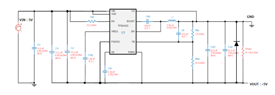
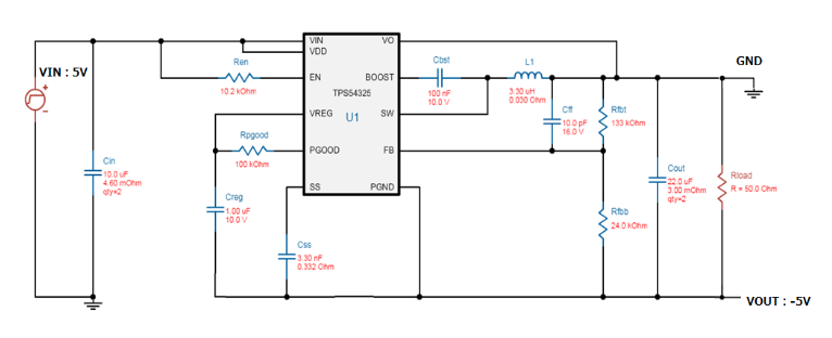
My customers are looking for the inverting power supply of the specification below.

Specification:5.0V ⇒ - 5.0V / 0.1A

We were promotioning negative power supply DC / DC and charge pump,

It was said that this time it can not be adopted unless it is a device with parts registration at the customer.

So TPS54325 is registration parts, I got a comment that it might be usable if proposed by inverting buck-boost circuit.

And, to consider, I was told that I would like examples of circuit diagrams on this device.

So please.

I changed the wiring based on the circuit simulating 10 V ⇒ 5.0 V / 0.1 A at WEBENCH and I was create the circuit diagram.

Would you please let me know if you can present it to customers with this circuit including the peripheral constant?

(Could you verify it ?)

※Correct it if there is a mistake, It'll be helpfull me.

Best regards,

Masumi Sekiguchi

  • Hi Masumi,

    The schematics looks good overall. Three comments and recommendation here:

    1) Please put one or two 10uF cap between Vin and -5V(PGND) and place it close to IC on PCB. This cap is very important to reduce noise and voltage spike on Vin.
    2) It is recommended to place one more 22uf cap at output.
    3) The PG pin here refers to -5V(PGND). In this case, it may not be used for EN signal for the next stage.

    I am not sure whether you would like to consider TPS563208 and TPS563219A as an option here. They are low cost version of this IC. Thanks!

    Best,
    Anthony
  • Hi Anthony,

    Thank you very much for your detailed answer.

    Please tell me addition.

    (I think that PG probably will not use, but I asked just in case.)
    You can not use PG's pull-up destination even if you use VIN or an external power supply.
    *Because the withstand voltage with between GND(5) pin to PG is decided internally at 6.5 V.

    Is this consider correct?
  • Hi Masumi,

    Yes, good point. The max rating for PG is 6.5V. So if you use external positive rails, the voltage high on PG could be higher than 6.5V. Maybe if there is a power rail below 1.5V, the power rail could be used to pull up PG. But need to check the EN threshold and choose the pull up resistor value wisely. Thanks!

    Best,
    Anthony
  • Thank you, Anthony.

    It's OK.

    While paying attention to that point,
    I will proceed with the proposal.

    Regards,
    Masumi Sekiguchi.
  • Hi.

    It seems that if you submit a proposal in TPS54325 about this thing, it will use.

    So,Again, we examined the proposing circuit.

    Please let me check 3 points !

    <Question 1>

    > 1) Please put one or two 10uF cap between Vin and -5V (PGND) and place it close to IC on PCB.

    > This cap is very important to reduce noise and voltage spike on Vin.

    Is this a bypass capacitor between VIN and VOUT?

    ※Equivalent to ① in the following circuit diagram

    <Question 2>

    See TPS62136 inverted reference design

    Design: TIDA-01423

    URL: www.ti.com/.../tiducy3.pdf

    URL(Japanese): www.tij.co.jp/.../jaju320.pdf

    Is a Schottky diode necessary between Vout and GND?

    ※Equivalent to ② in the following circuit diagram

    ※ For protection measures

    <Question 3>

    Can I use the PGOOD pin with GND?

    ※Equivalent to ③ in the following circuit diagram

    ※I know that PGOOD cann't be used with this negative power supply,is it better to pull-up to VREG 5 with 100 k?

    (want to dissconnest unnecessary resistance if connectable to GND)

    <Circuit Diagram>

    Best regards,

    Masumi 

    Sekiguchi

  • Hi.

    Can you comment on this?

    Best regards,

    Masumi Sekiguchi

  • Hi Masumi,

    Let me check on the reference design first and get back to you later. Thanks!

  • Can you give me an immediate answer on this matter?

    If it take time to confirm ....

    First of all, is there any problem by presenting it to customers with the following circuit?

    (I want you to check.)

    ※Although we will hurry, we will be able to interrupt if the answer is a problem.

  • Hi Masumi,

    Sorry for the late. Spend some time discussion Q2 with my teammates. 

    <Question 1>

    Is this a bypass capacitor between VIN and VOUT?

    Yes, it is a bypass. And with shorter trace from cap to Vin and Vout, the less parasitic inductance has on trace. This will give min voltage spike on Vin. 

    <Question 2>

    Is a Schottky diode necessary between Vout and GND?

    From the app note, the diode is used to prevent SW negative spike. It will help to protect the LSFET. However, talked with my teammate who build inverting buck boost before, he think diode is not a must. It is just a additional protection from the previous design and app note and became a well accepted knowledge later. For customer use, most of them did not put diode at output and we did not heard back any issues from them. In this case, diode may not be a must protection. But if you could accept one extra component, why not just leave it there.

    <Question 3>

    Can I use the PGOOD pin with GND?

    You could not use PG since PG is reference to -Vout in your application. You could build an external shifter circuit for PG function. Please check on section 2.2.2 in the app note: www.ti.com/.../slva469c.pdf 

  • Thank you for your answer.

    Thanks to your explanation, I was able to understand the role of each part.

    In other words, can you recommend to the customer with the circuit below which we sent today?

    (Is this circuit diagram OK?)

    Best regards,

    Masumi Sekiguchi

  • Hi Masumi-san,

    It looks good. Besides the PG function, there is no issue found.
  • Thank you for confirmation.

    I’ll discuss with customer about the PG function with the following two proposals.
    But is this consider "correct"?

    ① When PG is not used: Short to "-5V Node"
    ※ I want to know " is OPEN better for PG? " " is SHORT better for -5V's Node ? "
    ② When PG is used: Discrete design with reference to SLVA 469C level shifter circuit

  • Hi.
    Thank you very much for following me.

    PG isn't used as a conclusion confirmed, and the customer is undertaking the design review.

    So the question.

    ① Is this action OK to PG "Pull down to -5 V node"?
    (Please tell me if there is any other good action.)
    ② Is PowerPad also "5V pulled down to node" actions?

    Best regards,
    Masumi Sekiguchi
  • Hi Masumi-san,

    1. You could pull down PG to GND pin which is -5V node or let it float if PG is not used. There is no difference between these two methods. 

    1. PowerPad must connect the GND pin which is -5V node.