This thread has been locked.

If you have a related question, please click the "Ask a related question" button in the top right corner. The newly created question will be automatically linked to this question.

LM5116: Vout drops to half Vin when desired Vout is passed

Part Number: LM5116

Hello,

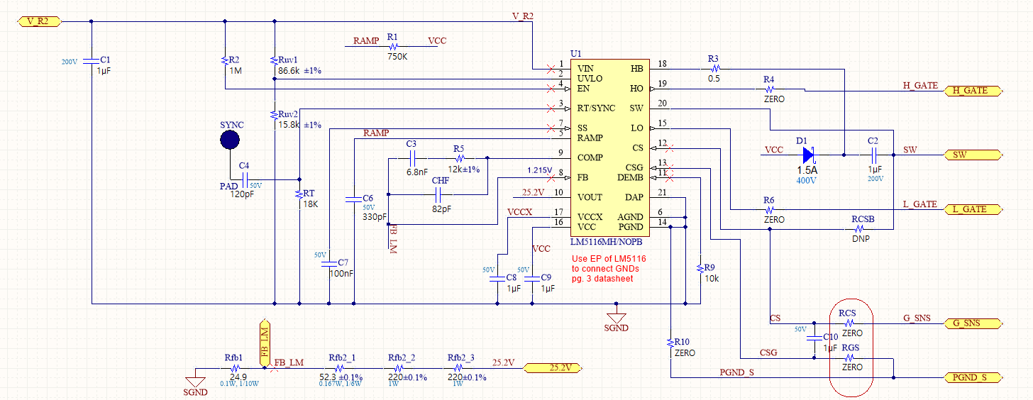
We are attempting to use the LM5116 to get Vout of 25.2V from Vin of 100V. As we increase Vin from 7V to 28V, Vout increases linearly until it passes 26V. When we increase Vin past 28V, Vout drops to 13V and no longer changes with Vin. We are very interested in knowing why this is happening.

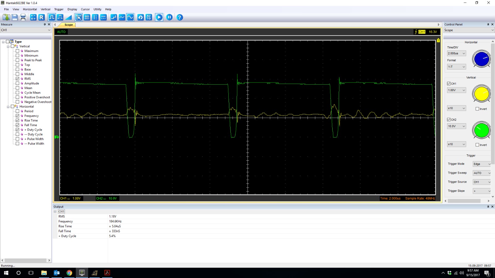
To help understand the problem, we found that the feedback voltage is very noisy (yellow) (green is the SW voltage):

We also found that as we approached the Vin that would cause the Vout to drop, the SW voltage cycle began skipping (green) (yellow is Vout), and Vout is greater than the targeted 25.2V:

Thank you for any help or recommendations.

Best Regards,

Phillip Angell


  • Hello Phillip,

    Please can you post your schematic?
    Along with the Spec you are trying to meet?

    Thanks.

    Kind regards,

    David.
  • Hello David,

    Thank you for taking time to take a look. We are trying to get 25.2V output and up to 20A. We are using 2 separate boards for the driver and MOSFETs connected through board-to-board headers. We used 2oz copper for the driver board and 4oz copper for the MOSFET board for heat dissipation. I mention this because one of my concerns is signal delay / integrity from using headers. Below are the two schematics, hopefully the port naming should be translatable.

    Thank you in advance for any help you can provide.

    Best Regards,

    Phillip Angell

  • Hello Phil,


    I checked your schematic, and I would like you to remove C10, if you are going to populate C10, make sure its no greater than 1nF and when insalled you need to have RCs and RGs installed, make them 100ohm each.

    Change RFB1 from 24.9ohm to 1k and caluclate the FB resistors from there...

    Change C6 from 330pF to 2nF
    Change Rramp from 750k to 100k
    Change R5 and C3 from 12k and 6.8nF to 10k and 22nF respectively.
    Change L1 from 2.6uH tot 22uH

    Can you check to see if things improve?

    Your concern regarding the Gate drive is understandable. I would check the timing and compare the outputs of the Device to the output to the gates of the FETs. You can place RC's delays (with a Back Biased Diode) to the inputs of the driver, to ensure you dont run into issues. You can then tune the RCs accordingly, if needed?

    hope this helps?

    kind regards,

    David.
  • Hello David,

    I was able to make most of the changes you recommended:

    1. Removed C10
    2. Changed Rramp to 100k
    3. Changed R5 and C3 to 10k and 22nF
    4. Changed Rfb1 and 2 to 1k and 15.8k, respectively (this reduces Vout to 20.4V)

    However, due to space constraints and immediate availabilty, I am unable to increase the inductor with the desired current rating. I have instead replaced L with a 18uH / 1A inductor for testing, and C6 has changed from 330pF to 1.2nF. Because the inductor is only rated for 1A, I have put a 33 Ohm load at the output to limit the current.

    We also increased the switching frequency from 180kHz to 300kHz (by reducing Rt to 10k), and saw some improvement.

    I did check the timing between the gate output of the driver and the gates of the MOSFETs and found there was no noticeable delay, so the use of the headers to connect the driver to the rest of the circuit does not seem to be an issue.

    When I test the circuit with these changes I get an output of 21V (21.1-21.4) when Vin is between 24V and 28V. After 28V, the output begins to fluctuate similar to the symptoms we got before it failed previously. (Yellow is the high side MOSFET gate, green is Vout)

    Thank you in advance for any insight you can provide.

    Best Regards,

    Phillip

  • Hello Phillip,

    Thanks for the response.

    Have you followed the layout guide lines in the datasheet.  To make it easier for you.  Please refer to the attached and let me know if the layout is in accordence with the recomendations therein?

    5165.lm5116 Flour Plan.pdf

  • Hello David,

    The layout guidelines in the datasheet were followed as closely as possible, but I was unaware of the additional floorplan.

    There are a few small variances from the floor plan you linked:

    1. Vcc GND is not connected directly to PGnd, but connects directly to the EP, which connects to both AGnd and PGnd.
    2. Vsw is not as small as it could be, but it is not large either.
    3. CSG is connected to PGnd locally, on the separate driver board and not directly next to the Rsense by the MOSFETs.
    4. Rsense/MOSFET loop is not kept small/tight.
    5. Lastly, Vin has aluminum caps for most of the capacitance, and one ceramic cap right next to the driver.

    Would it be possible to set up a phone dialog regarding the design?

    Best Regards,

    Phillip

  • Hello Phillip,

    There are a couple of items that you list above that are critical. I think having a phone conversation would be most efficient at this point.

    Please email me so we can exchange details and connect on a call.

    David.Baba@ti.com

    Look forward to hearing from you soon.

    Keind regards,

    David.
  • For those that happen upon this thread looking for answers, communication with David proved successful in answering question we had regarding the LM5116 operations.

    There were a few smaller issues regarding PCB layout (highly recommend following the floor plan posted above), but three issues stood out as the key elements in the solution.
    1. Keep the MOSFET / Rsense / Cin loop as small as possible (see floor plan)
    2. Output inductance was too small, stick to recommended ratings.
    3. LM5116 can only supply limited current for Vcc. For most designs this is not an issue, but if you require MOSFETs with a sufficiently larger Qg, check the average current required to drive the gates. If you are over the limit, use an external Vcc; one of the reference designs on the LM5116 page uses this approach.

    Thank you David for all your help.

    Best Regards,
    Phillip