This thread has been locked.

If you have a related question, please click the "Ask a related question" button in the top right corner. The newly created question will be automatically linked to this question.

TPS53647: Configuration for 60A current requirement

Part Number: TPS53647
Other Parts Discussed in Thread: TPS40428, TPS56720, TPS65400

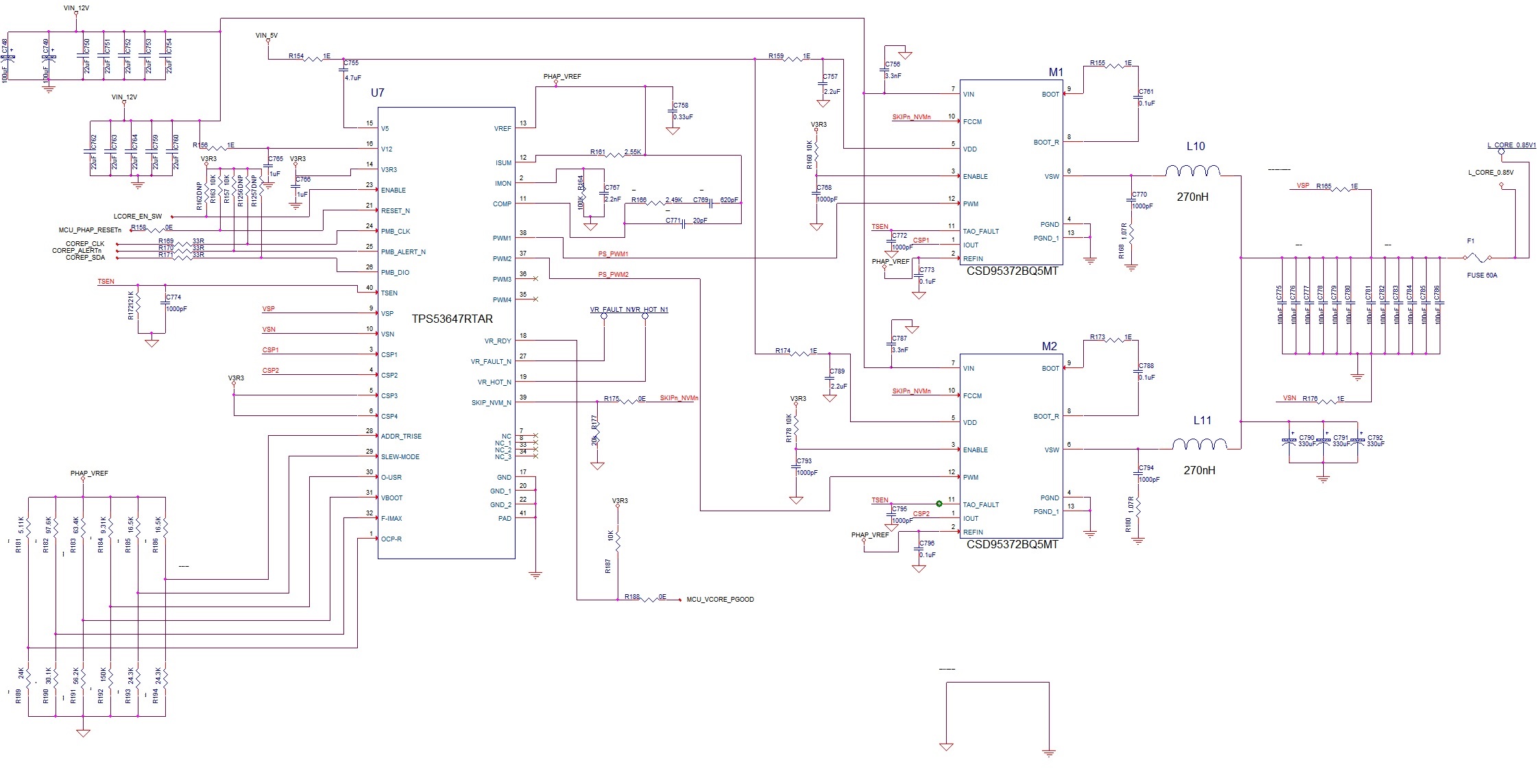
We are planning to use TPS53647 in our application :

VIN = 12V 
Vout = 0.8V to 0.9V with 0.85V (nominal)
Current = 50A Max
Programmable through I2C
Output voltage should be programmable
Enable option

I think it supports 120A current with all four phase.
Do i need to use all four phase for 50A current requirement?
Is it compatible with I2C bus interface?

  • Hi Rahul,

    TPS53647 seems like it would be a great fit for your application when it's paired with one of TI's Smart Powerstages. The controller is fully PMBus compliant so you can change the output voltage while also receiving voltage, current, and temperature telemetry. 

    For a 50A application you don't have to keep all four phases active or place four powerstages. On phases 3 and 4 you can simply tie the CSP3 and CSP4 pins to 3.3V and they will be disabled.

    If you have any other questions please feel free to ask.

    Cheers,

    Carmen

  • Is it compatible with I2C bus interface?

  • Hi Rahul,

    Yes, PMBus is an open protocol extremely similar to I2C. If the customer is using I2C they'll have no problem implementing PMBus.

    Thanks,

    Carmen
  • If i use two phase only phase 1 & 2 for 50A current requirement.
    1. Do i still need to place phase 3 & 4 components? what would be the state of PWM and other pins of Phase 3 & 4 ?
    2. Can i set default output voltage 0.85V at power On and after that output voltage can be programmed b/w 0.8 to 0.9V using I2C bus ?
    If you compare my application which one WILL better between to TPS53647 & TPS40428 ?
  • Hi Rahul,

    No, you do not need to place any components for phases 3 and 4 in a 2 phase application. Tje PWM pins would be left floating and each CSP pin would get tied to the +3.3V supply.

    Yes, the TPS53647 has a register for VBOOT and another register you can write to to change the output voltage once the pat is up and running. Simply set VBOOT to 0.85V and then have whatever is talking to the regulator through PMBus send the appropriate VOUT command. There are also pinstrapping options that can configure the startup configuration as well to give you more options.

    After just a quick look at the TPS40428 datasheet I think the TPS53647 would be a better fit for your application. It looks to have a more robust modulator which is easier to compensate and from what it sounds like you aren't looking for the AVSBus functionality. TPS53647 can also be configured from 1 to 4 phases making it more flexible than the TPS40428 should your current design needs change or you want to reuse the same controller with minimal rework in a new design.

    The only thing that separates the two that you would have to consider, in my opinion, is whether or not you want to use smart power stages. TPS53647 is only compatible with TI's power stages while the TPS40428 can use either smart power stages or traditional driver-MOS options. Smart power stages offer better current sharing information, no DCR loop tuning, smaller PCB area, and an optimal driver/FET combination than a discrete solution. What are your top design considerations?

    Thanks,

    Carmen
  • Can I set boot voltage 0.85V using external resistor without programming in the power ON time and then I could change output voltage using I2C?

    Actually, i am using three ICs in my design first TPS65400 second TPS56720 & third will be TPS53647 and I want to power ON all three ICs using an external power sequencer for the boot time only. means all ICs should generate supplies in the boot up without programming.

  • Hi Rahul,

    Yes, as I mentioned above there are pin-strapping options to set the boot voltage and various other parameters on the IC. The boot voltage is set using a resistor divider on pin 31 between VREF and GND. You can learn more about it on page 97 of the datasheet. Any voltage listed in the VID table should be able to be programmed as the boot voltage.

    Thanks,

    Carmen

  • Hi Carmen,

    When look into the datasheet at page no 97 for boot voltage setting using external resistor. I am not seeing the option for 0.85V voltage setting using external Rboot resister and Vboot voltage bits. In the table 79 only VBOOT = 0.797V ± 20 mV & VBOOT = 0.903V ± 20 mV are mentioned but if if i want to set voltage for 0.85V than what would be setting for resistors ?
    Please guide me..
  • Hi Rahul,

    The voltages in Table 79 are voltages for the VBOOT pin, not output voltages. Any output voltage can be programmed from the VID Table (Table 1). To program you 0.85V on startup you would have to follow these steps:

    1) Choose the appropriate VID code from Table 1. It sounds like you don't need voltages >1V so either the 12.0 or 12.5 spec will work unless there's some aspect of your design we haven't discussed yet.

    2) Choose RBOOT from pin 31 to ground to set B3, B2, B1 of that VID code

    3) Calculate the resistor from Pin 31 to Vref (1.7V) to set the voltage on pin 31 to the approriate level for bits B7, B6, B5, B4

    4) Make sure the last bit, B0, is set correctly when picking the resistor from pin 28 to ground. This resistor sets both the final VID code bit and the slew rate of the output voltage (Table 74).

    Thanks,

    Carmen
  • Hi, Carmen

    I have completed the Schematic.

    Please have a look and comment if any 

  • Hi Rahul,

    Please see my comments below on the schematic.

    1. You don't need AGND for the power stage components
    2. If you are using AGND for the controller side of things then the controller ground has to be AGND
    3. R161 = 0 if you don't need a dc load line
    4. Power stage VDD resistors R159, R174 should go to VIN_5V directly
    5. Power stage enable lines should pull up to power stage VDD pins
    6. C773, C796 = DNP
    7. Make sure in layout to place 3x22uF caps near each power stage input
    8. Resistor on Pin 40 of controller, TSEN, should be DNP
    9. Are the FAULT# and VRHOT# pull ups located elsewhere?
    10. Place a 22pF cap from VSN and VNP to GND. Place a place holder cap between VSP and VSN in case it's needed during validation
    11. Are catch resistors to the output and GND all that are needed or should feedback lines from the CPU also be placed?

    Let me know if you have any questions.

    Thanks,

    Carmen

  • Hi Carmen,

    Point no 11 not understood?

    Pls clarify

  • Hi Rahul,

    Currently only R165 and R176 are providing feedback from the output node to the controller. Typically processors will have voltage feedback points that get fedback as well. These feedback lines are directly connected to the VSP and VSN pins. Then R165 and R176 would be some small value like 10Ω and provide a local connection to VOUT. 

    This way you get tighter regulation at the CPU which is where you want VOUT equal to the set voltage but can still power up the board during validation without a processor in place.

    I was simply asking if the local output connections were all that are needed.

    Thanks,

    Carmen