This thread has been locked.

If you have a related question, please click the "Ask a related question" button in the top right corner. The newly created question will be automatically linked to this question.

LM5022: Isolated DC/DC, audible noise

Part Number: LM5022
Other Parts Discussed in Thread: PMP20551, LM3481, , LMV431

Hi here,

The forum didn't allow me to select the Isolated DC/DC Forum, I do apologize. I used Webench to help me design a Isolated DC/DC Converter, I added in some additional filtering, some bulk capacitance on the input, a LC filter on the output and a over voltage input protection cutoff circuit stolen from PMP20551.
The design requirements were:


Vout:12v

Iout:0.9A

Vin 20-50V

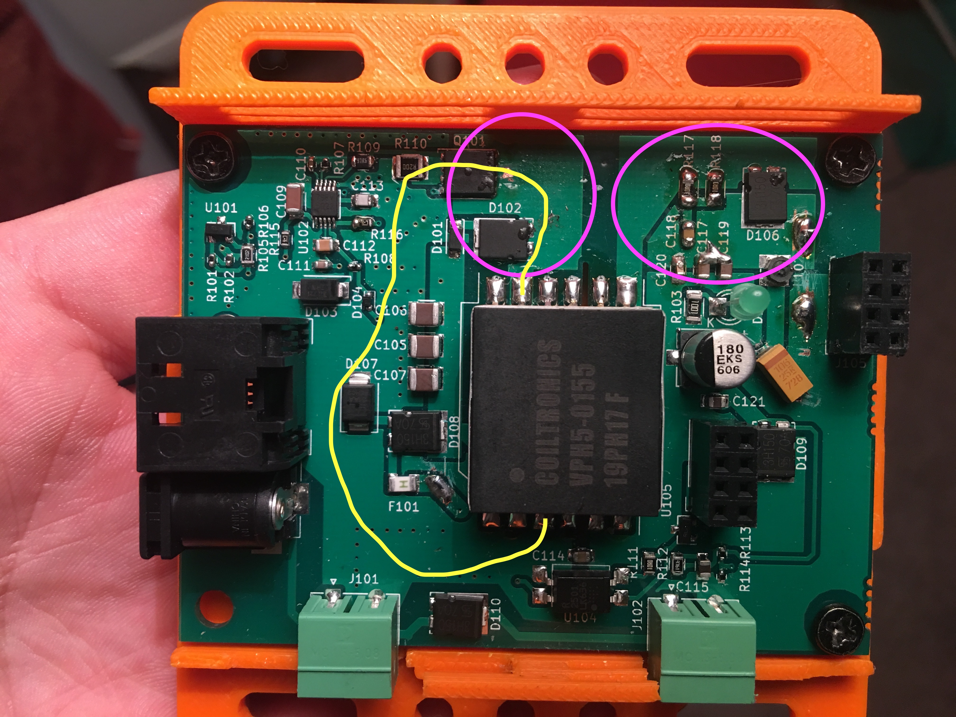
Attached is the Schematic, as well as the PCB layout.
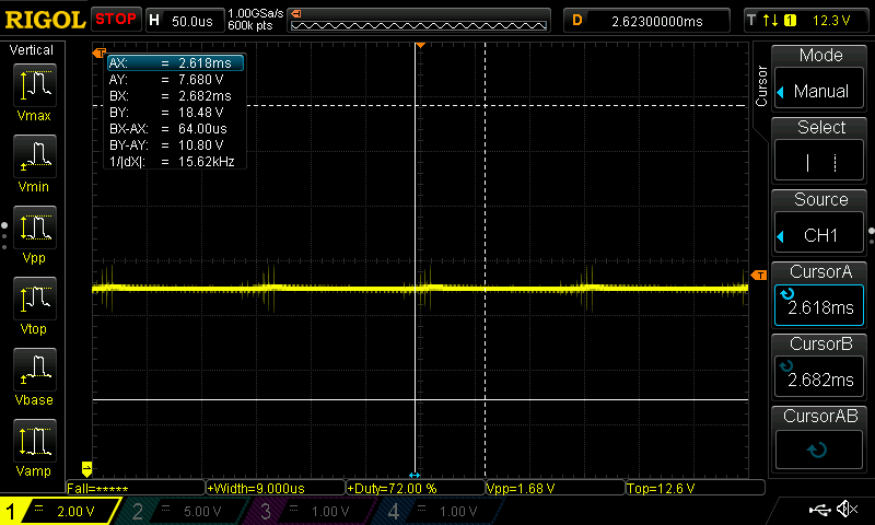
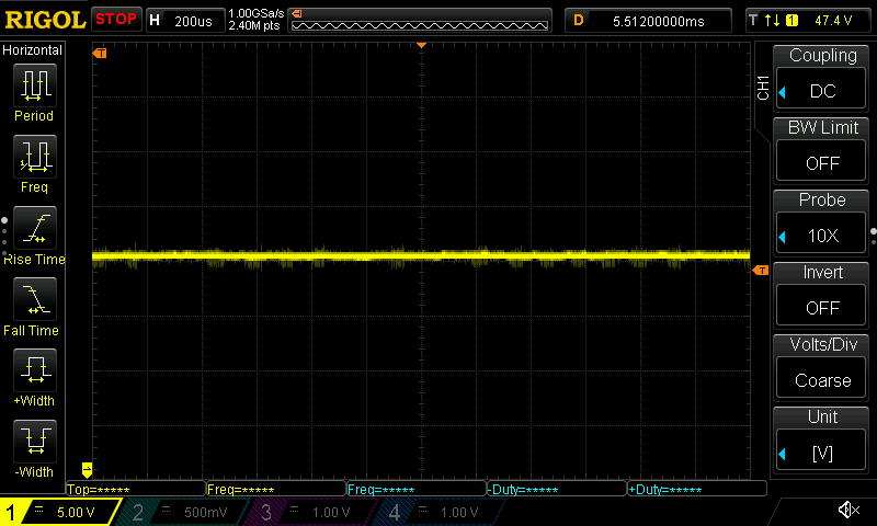
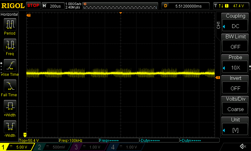
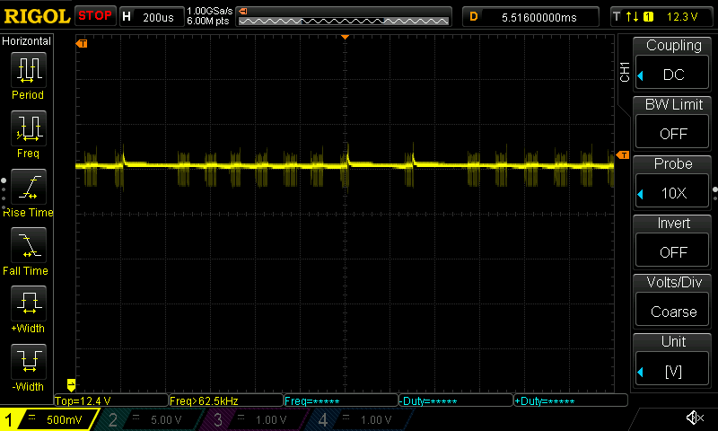
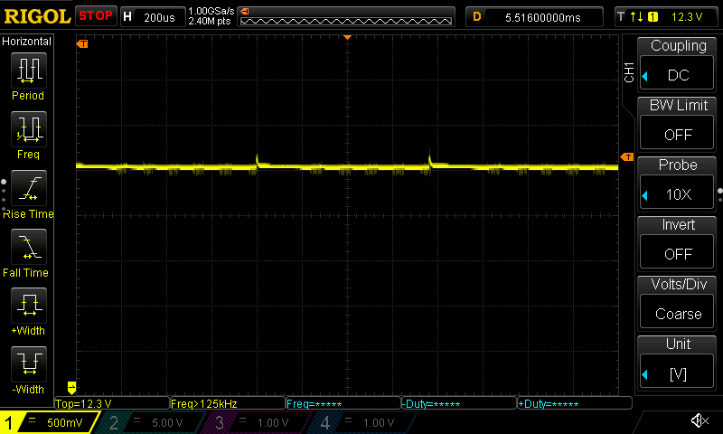
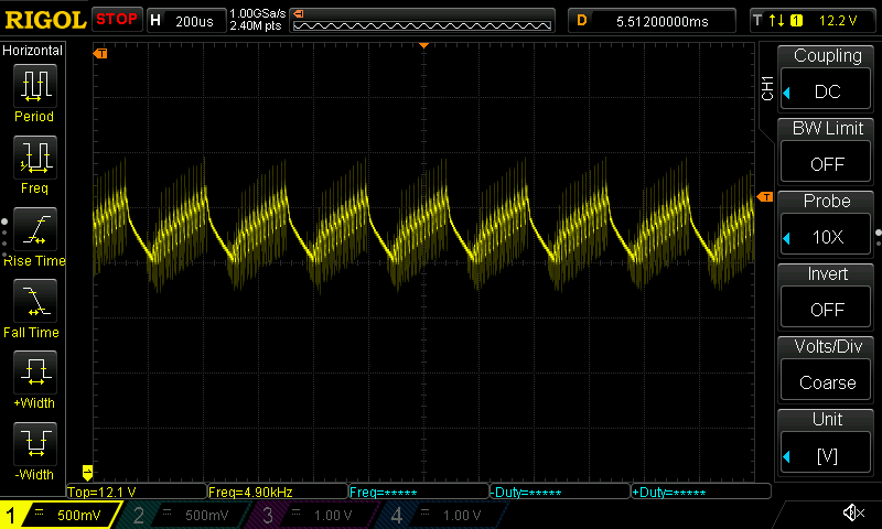
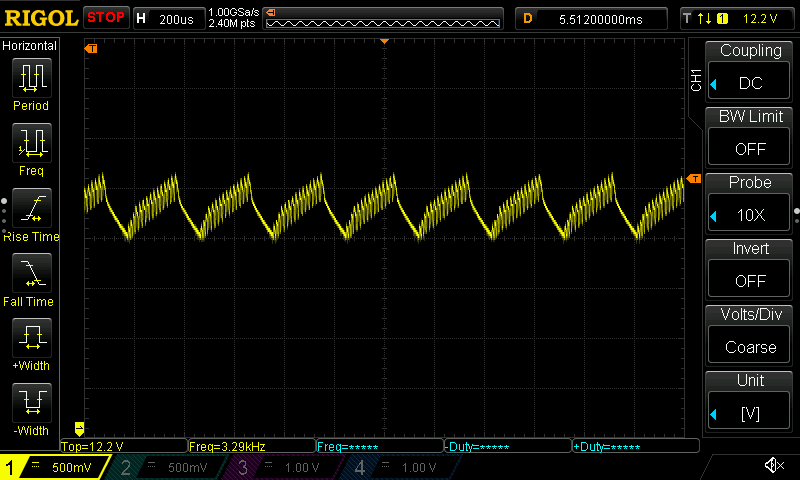
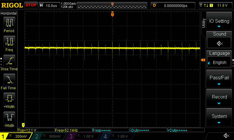
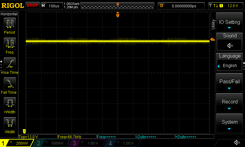
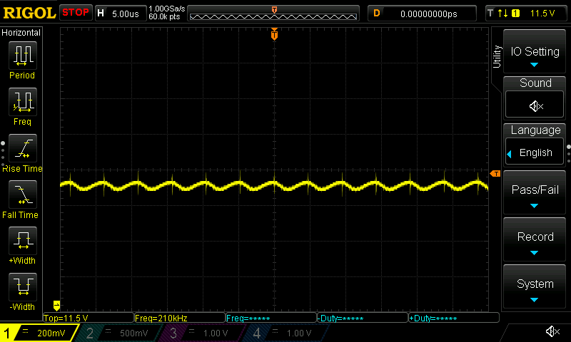
There was a tiny amount of noise on the output, so I added a 100uF tantalum I had laying around on the output, and replaced one of the 22uF MLCC output caps with a 0.1uF which seemed to solve the problem. One of the majorly annoying perks of the design was an audible high pitched noise, which was quiet (but noticeable, more a fuzz sound) at no load, and when a load was applied it got much louder. I attempted to locate the source of the noise with a rolled up piece of paper, but was unsuccessful in pinpointing the source. Applying firm pressure to the transformer seemed to dull the sound. (The transformer I used was a Coiltronics VPH5-0155-R with 2 windings in series for the primary, secondary and auxillary).

The attempts made to try and reduce/get rid of the noise include :
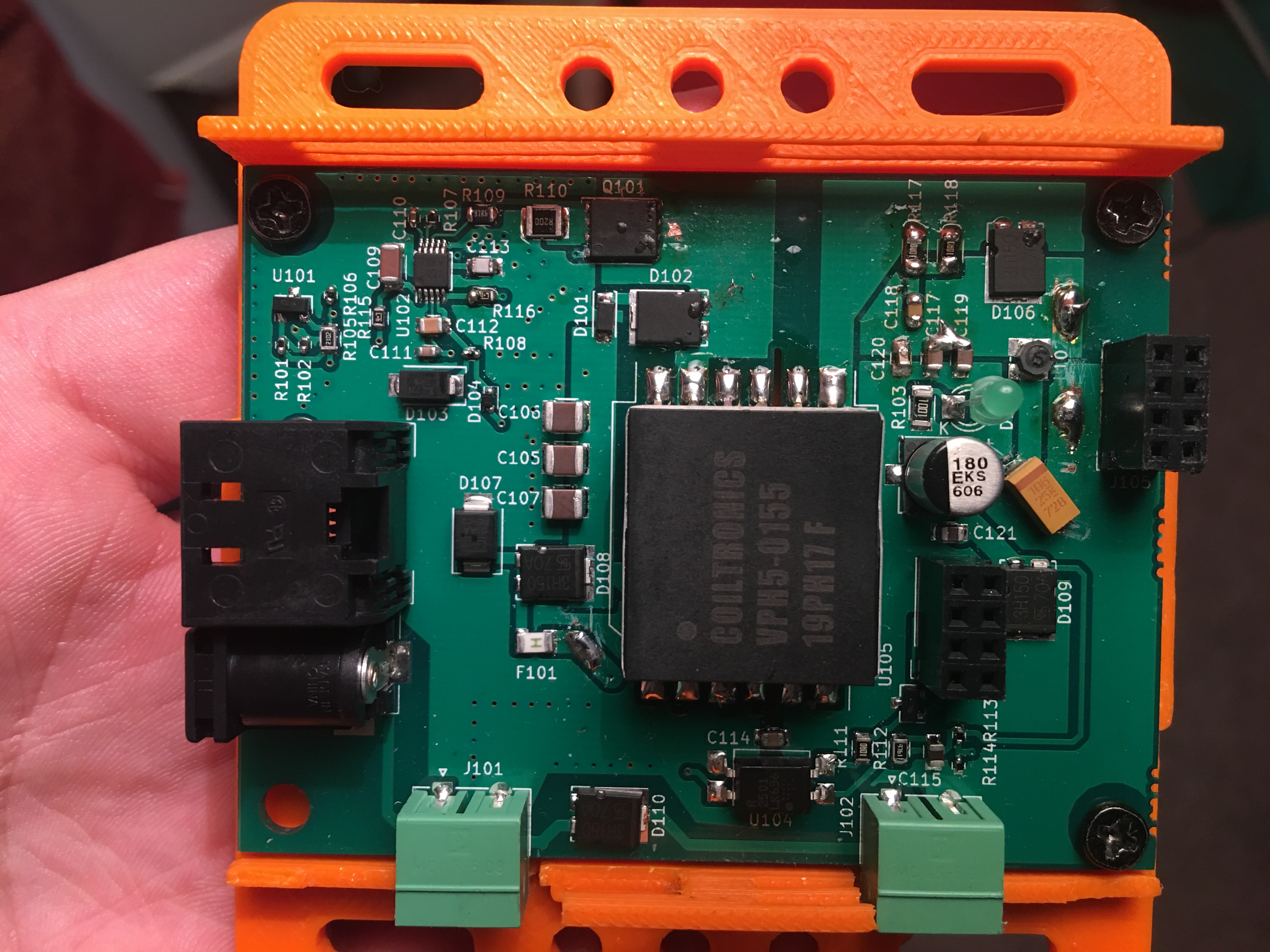
  • Extra filter capacitors after the output diode
  • RC snubber across the output diode 
  • Bypass the resistor on the Gate of the mosfet

Which all didn't reduce the noise, but did change the audible frequency slightly.
So I'm wondering if its a poor PCB layout, or I've somehow made it unstable or that there will always be noise due to the transformer.

8468.schematic.pdf

  • The engineer in charge of this part will reply to you in the new year.
  • You're welcome, wait in patient.

  • Hi Mitchell,

    Is the audible noise present at all input voltages? Is there a specific input voltage range where you can hear it? What snubber component values did you test across the output diode?

    My first thought is that there might be an instability issue with the LC filter on the output. Can you look at both sides of L102 to see if there is any low frequency ringing? Please also check the input voltage to make sure that it is not ringing as well.

    Regarding the layout, I would suggest trying to decrease the SW node size. This can cause a lot of issues including audible noise. The high di/dt current loops look large too. It would be good to have these shrunk down.

    Thanks,

    Garrett
  • Thanks for getting back to me Garrett,

    So my current voltage supply is a bit limited, the current voltage range I can test is 40 to 50v. With a voltage of 40v, the audible noise does seem a bit lower in frequency and slightly quite (but not by much). So I originally had no snubber, then I added in a 10nF and two 10R resistors in parallel (5Ohms) this is all I had on hand at the time. 

    Attached below is two screen shots I took of the output, unfortunately I can't remember exactly which one was under load, or if it was measured before or after the LC filter. I will be able to make measurements in a week or so.

    I realized after the PCB's were ordered that the switch node size was a tad on the large side. Also attached is a better view of the layout and a quick drawing of what needs to be improved in terms of layout. I just realized that the switch loop is also quite large (the yellow line).

  • Hey Garrett Roecker,

    here are some scope shots. The resistive load is a 15 Ohm resistor

    Input, no load 48V

    Input resistive load 48V

    Before L102, no load

    after L102, no load

    before L102, resistive load

    After L102, resistive load

  • Hi Mitchel,

    I just realized that the isolated feedback doesn't have a capacitor between pin 3 of the voltage reference and the feedback resistors. Please try adding 100nF here. It looks like this might be a stability issue since there is about 500mV of ripple on the output. Another though would be to move the regulation point before L102. This guide is for the LM3481 but can be uses as a good reference for isolated feedback design.

    Thanks,

    Garrett

  • Good find with the capacitor, not to sure how I managed to miss that!! So I added the capacitor in, I also moved the regulation point before the inductor and removed the snubber (for now). The noise was still present, so I added two 100uF electrolytic's to the output and the noise pretty much disappeared, but is that sawtooth output voltage waveform typical for a flyback?. Attached are the scope shots.

    Output, no load

    Output, resistive load

    output no load with output caps

    Output, resistive load with output caps

  • Hi Mitchell,

    At no load it will be common to see a little more ripple. That is because the LM5022 will skip pulses as needed. Changing the output capacitance indicates that some of the noise might have been due to the output EMI filter impedance. Glad to hear you got everything figured out.

    Thanks,

    Garrett
  • Hey Garret,

    I ended up redoing the board. Reduced the size of the nodes as suggested added extra output capacitance and included the compensation capacitor that I had originally missed out on.

    The noise returned... I removed all the filtering capacitors on the input and output, the noise was still present so I replaced them. I then swapped out the 150nF compensation capacitor (what was recommended by webench) for a 100nF. The noise disappeared with a light load but was still there with a large load. After a short while of testing with the light load, the circuit shutdown. I traced it back to the Auxillary diode, it's wasnt a full short circuit, but was conducting both ways. I replaced it with a spare and it was up and running again.

    The diode is:

    industrial.panasonic.com/.../DB2S31600L_E.pdf

    This was recommended by the Webench designer. Rating of 30V

    The diode ended up burning out again, so I replaced it with a 1n4148 and measured the voltage before the diode with the scope.

    The image below is with no load:

    The image below is with a load


    So I'm guessing the compensation circuit is unstable? 

  • Disconnected the compensation circuit from the output of the secondary diode. I used a 15Ohm load resistor. Attached is an oscilloscope screen shot of Vout. There was no audible noice, complete silence.

  • I looked at your schematic and I did not see any loop compensation network. Please refer to the webench generated schematic and add the compensation around the LMV431, and also add a series resistor of 1k to C111 and increase C111 to a about 470nF (this RC is a guess which can be adjusted if you wish).