This thread has been locked.

If you have a related question, please click the "Ask a related question" button in the top right corner. The newly created question will be automatically linked to this question.

tps2490: EN input does not affect PG. PG cannot be used for downstream control of regulators contrary to statements in the datasheet

Part Number: TPS2490
Other Parts Discussed in Thread: LM5069

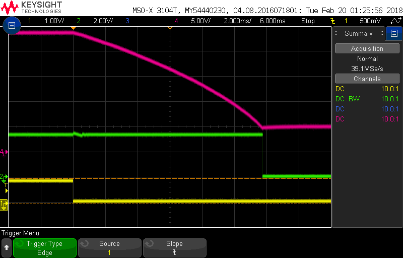
I have proto boards using the TPS2490 where the PG is used for downstream control of regulators as advertised.  Going by the datasheet statement in SLVS503E,  PG is false (low) whenever the voltage across the pass MOSFET exceeds 2.7V  or UVLO is active.   In the screenshot below, the PG does not react to either of the stated conditions (yellow is EN input, green is PG output, Red is the MOSFET source voltage).  Per the datasheet statement in 7.3.9,  PG should have gone low at where the source voltage crossed 21.3V down where Vds exceeds 2.7V (about 2msec following EN falling edge), no mention of the delay.

More disturbingly, the functional block diagram at 7.2 shows EN and UVLO AND'ed together to produce the Enable signal, but no connection to the PG signal path in support of the statement in 7.3.9.

Is there anything not shown in 7.2 that bypasses the 9msec timer and trips the PG on power down?  I've got switchers going into starvation since the PG does not reflect the state of the power at the MOSFET source.  I'd have to add a boatload of capacitance on the load side to keep them from starving for 15msec (maximum timer spec).  PG cannot be used for downstream control of regulators like this.

  • Rick,

    The DS looks to be correctly worded and depicted in the block diagram. PG section 7.3.9 states that 'Both Vds rising and falling are deglitched {with 9ms nominal deglitch you see on your scope shot} while UVLO is immediate'. You don't show Vin so you don't have UVLO depicted, but you will find it is immediate. Make sure you are referring to UVLO as it is tied to Vin, not Enable in your assessment. The scope shot looks normal and per DS with deglitch time.

    The Enable in the block diagram is an internal Enable, not the external 'EN' enable. Both UVLO and EN inputs have to be in the correct state before the IC will turn on the Gate.

    The 9ms deglitch cannot be be disabled.

    Brian
  • Thanks for your reply. Vin remained steady at 24V, so I understood that UVLO would not activate under my test conditions. I also understood that the internal ENABLE is not exactly the EN input signal.

    The statement in 7.3.9 that UVLO directly de-asserts PG is not depicted in the the function diagram 7.2. It's easy to make the incorrect assumption that the internal ENABLE signal is the direct control path for UVLO, and, by it's logic AND depiction with the EN input, that EN would have the same effect. It would also make sense to stop filtering for transient events during an intended shutdown via EN.

    Looks like I'll have to add an external voltage monitor on the load side and use the output as a "true" PG to the downstream converters. Adding the capacitance needed to keep the highest regulator (12V) from starving for 15msec is not a practical solution for us.
  • Rick,

    If you have the flexibility, the LM5069 is a similar class high voltage hotswap that should function more to your needs wrt PG and may be worth a look into. In some ways, I prefer it to the TPS249x series. If you do use it, the dv_dt control is a little different with a BJT used. The BJT circuit limits the energy into the internal gate pull down FET and is there for long term reliability if multiple faults occur.

    Brian