Hello,
I'm using a
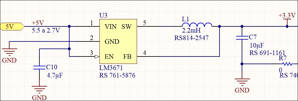
LM3671MF-3.3NOPB
in one of my designs, from 5V to 3.3V. Power consumption is around 300mA , the device is buzzing (sound can be hear), and sometime goes to a short, and an infrared camera shows a lot of heat (of course)
The output voltage should be 3.3V and is 2.9V, with triangle ripple at 10Khz, and 0.4V amplitude.
The self is 74404054022 from wurth electronic
Enable pin is connected to the input pin directly. Could it be the issue ?
I have replaced the device two times and no improvement. I followed the recommendations
If I put a scope probe (not active) on pin 5 SW, the device is becoming completely crazy. I did not expect a 15 pf probe to mess up the device to that level.
Regards,
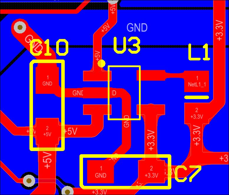
PCB ->