This thread has been locked.
If you have a related question, please click the "Ask a related question" button in the top right corner. The newly created question will be automatically linked to this question.
Hi,
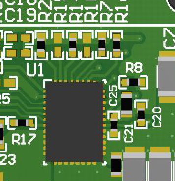
In Rev. B, a capacitor of 10 to 100 nF is recommended for Pin 25 (PVIN) to Pin 27 (GND).
In the layout guideline, it is recommended to place it as close to the IC.
However, to place the decoupling capacitor of Pin 26 (VDD) to Pin 27 (GND) as close to the IC is also recommended .
How should we place a small capacitor of Pin 25 to Pin 27?
Best regards,
Yuto Sakai
Sakai-san,
Connect the input capacitors ,including HF bypass capacitor (10 t0 100 nF) from the PVIN pins (21-25)to the PGND pins (13-20)and the VDD bypass capacitor directly across Vdd (pin 26) and GND (pin 27) as shown below. Place the small HF bypass capacitor (10 t0 100 nF) closest to the IC as shown:
Hi John-san
Thank you for your reply.
When the revision is changed(Rev.B), a description has been added that a capacitor of 10 nF to 100 nF is recommended between Pin 25 (PVIN) and Pin 27 (GND) as follows.
How is this capacitor recommended to put? Is it OK next to VDD Bypass capacitor?
As the capacitor between Pin 25 (PVIN) and Pin 27 (GND) is also recommended near the IC, please tell us the recommended layout.
Best regards,
Yuto Sakai
Sakai-san,
The PVIN bypass capacitor placement will have priority. The routing under the component will only be an issue if you split VDD as a different voltage than PVIN. If they are the same the connection is simplified. You can tie pin 25 to pin 26 directly at the IC.
Hi John-san,
Thank you for your reply.
If VDD and PVIN are the same voltage, I think that wiring will pass under C25.
I attach the image below, so would you please check my question?
TPS543C20_layout plan.pdf
Best regards,
Yuto Sakai
Hi John-san,
Thank you for your reply.
When PVIN and VDD are common rail, I understood that the VDD capacitor is close to the IC and the PVIN-GND capacitor is immediately next to it.
When PVIN and VDD are common rail, we understood that the VDD capacitor is close to the IC and the PVIN - GND capacitor is immediately next to it.
Also, since the previous post has disappeared, can you show me the new EVM user's guide?
Best regards,
Yuto Sakai
Sakai-san,
Not that I know of. The EVM allows for the possibility of separate supplies for PVIN and VDD.
Hi John-san,
Thank you for your reply.
When wiring PVIN-GND capacitor and VDD-GND capacitor with separate trace, which capacitor should be placed in the IC closest?
Could you confirm with the TPS543C20 team?
Best regards,
Yuto Sakai
Sakai-san,
The application engineer wants to know your Vin, Vout and Iout to best place the capacitors. Just FYI, going forward I will no longer be supporting TPS543C20.
Hello Sakai-san,
My name is Kit Nguyen. I am supporting this device and able to help you further. John had forwarded all the information and has been communicating with me internally Ti. I understand your questions on VDD bias capacitor and Vin bias capacitor. Here are some feedbacks:
1. Vin capacitors:
1a) I saw you already a small capacitor which next to pin 20 and 21. This capacitor (pin 20/21) has more priority to reduce the ringing on the drain to source of both upper MOSFET and lower MOSFET. Also, this capacitor will also reduce the ringing spike during the turn-off of upper MOSFET.
1b) Pin 25 to 27 capacitor: this capacitor will help to reduce the duration of ringing. Please see attach waveforms for comparison with and without 10nF at those two pins. The waveform shows Vin to SW voltage during turn-off of upper FET with 12Vin/0.9Vin/500kHz/35A conditions (Blue trace--No 10nF at pin 25/27; Red trace--10nF at pin 25/27). This capacitor will help reduce the Vds-SW voltage.
2. VDD capacitor: The purpose of this capacitor is supplying the charge to the VREG (output of LDO) and an input of LDO. I suggest to route the GND of this VDD capacitor to the pin 26 directly as the shortest distance to thermal pad. Can you use this cap as same as in the EVM user guide CAP, CERM, 1 µF, 25 V, +/- 10%, X5R, 0402 (Murata GRM155R61E105KA12D)? This capacitor can be place next to pin 25 and 26. Then pin 25 to 27 capacitor. From your placement layout, it looks like there is enough space between IC and pin 25/27 capacitor for another 0402 cap. Also, the ground side VREG capacitor needs be same ground plane as those capacitors as drawn suggestion.
Questions: What is your design condition: Vin, Vout, output current and Fsw? I can guide you further to better optimize the layout.
Kit
Hi Kit-san,
Thank you for your reply.
The design condition is Vin=12V,Vout=0.9V,Iout=11A,Fsw=500kHz.
Patterns are wired under the Pin 25-27 capacitor in the EVM User's Guide and can not be wired in the same way.
Drawing a pattern under the part is prohibited by customer rules.
If there is a better layout plan, please let me know.
Best regards,
Yuto Sakai
Hi Kit-san,
I'm sorry for bothering you.
There are other designs using TPS543C20, and I also want to consult the layout.
Which of the VDD and Pin 25-27 capacitors should be placed closest to the IC in priority?
The designs condition are as follows.
・Vin=12V,Vout=0.72V,Iout=68A(2Phase),Fsw=500kHz
・Vin=12V,Vout=1.2V,Iout=22A,Fsw=1MHz
Best regards,
Yuto Sakai
Hello Sakai-san,
Since the output current is only 11A, you can put Pin 25/27 capacitor at bottom layer. And, place VDD bias capacitor next to the IC at pin 26/27. Also, TI has released 25A version (TPS543B20) of this family. TPS543B20 has 25V FET rating in comparison with 20V FET rating in TPS543C20.
Kit
7356.Doc1.docxHello Sakai-san,
I was not clear enough in the previous document file on the layout of those capacitors.
If the customer can use 0402 size for VDD capacitor, this capacitor can be next to the pin 26/27. Then, the trace connects to VDD can be bottom or internal layer and via up to connect to the cap. As result, no trace go through the Vin capacitor. Please see attach picture.
If the customer can not route as suggest above:
Vin=12V,Vout=0.72V,Iout=68A(2Phase),Fsw=500kHz: place the Vdd cap at bottom layer and Pin 25/27 next to the IC. Please allow ground side of VDD cap and Vin pin 25/27 cap join together through at least 2 vias with GND plane.
Vin=12V,Vout=1.2V,Iout=22A,Fsw=1MHz : Place pin 25/27 cap at bottom and Vdd cap next to pin 26/27. Please allow ground side of VDD cap and Vin pin 25/27 cap join together through at least 2 vias with GND plane.