This thread has been locked.

If you have a related question, please click the "Ask a related question" button in the top right corner. The newly created question will be automatically linked to this question.

TLV742P: at what point is a heat sink required?

Part Number: TLV757P

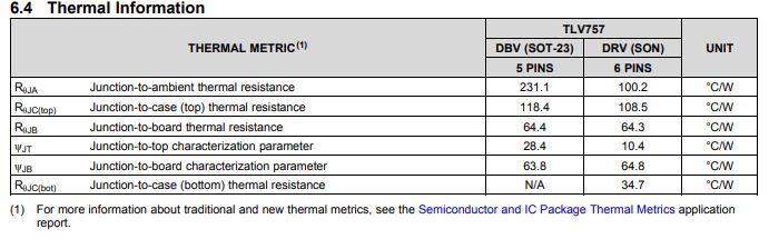
I am considering using a TLV75733PDRVR LDO to drop 4V to 3.3V while driving up to 1A, thus needing to dissipate around 0.7 watts.  Would an additional heat sink be required in this situation, assuming the PCB provides a large copper plane well thermally connected to the TLV757P's thermal pad?  Page 18 of its spec sheet was kinda vague on this.  I am using a 4-layer FR4 board with 3 oz/ft^2 copper on its outer layers and otherwise standard PCB fab technologies.  I can provide an array of plated vias (how many do I need?) under the device to conduct heat from the top layer to the bottom layer.  How big of a total area of copper should exposed on the top and bottom layers to be ok with this amount heat dissipation?  I don't know how to calculate this; any pointers would be a big help.  Thanks heaps in advance.

Also, how does the answer change if this LDO were used to drop all the way down from 5V (again, providing 3.3V at up to 1A), thus needing to dissipate around 1.7 watts?  

  • PS - Page 6 of www.ti.com/.../snva419c.pdf indicates the following rule of thumb when working without a heat sink "at least ... 2.37 in^2 of area to dissipate 1 watt of power for a 40°C rise". Is that generally what I should work with here?
  • Hi Thomas,

    There are many application specific factors that determine when additional heatsinking may be required.  Power dissipation and board layout are definitely two of them; however, ambient temperature and proximity to other heat sources cannot be discounted.

    The primary heatsink for an LDO such as TLV757P is the copper connected to it in the PCB and in particular the GND plane.  As such, you will want to maximize the copper connected to the LDO within your specific application constraints.  By connecting the NC pins to GND and placing a couple vias in the thermal pad you will increase the GND plane at the LDO.  You can also place a couple of GND vias close to the LDO to help transfer heat down to other layers away from the LDO.  

    As to choosing how many vias there are a few things to consider.  While the copper will help transfer the heat to other GND layers, keep in mind that unless you pay extra, there is a hole in the middle of the via.  For the vias in the thermal pad, this hole can cause the via to wick solder away from the thermal pad connection to the PCB reducing the effectiveness of the thermal pad.  As such, I would only place two vias in the thermal pad itself.

    While your layout will have better thermal performance than the JEDEC hi-k board, we can still use the Thermal Information table as a first pass for thermal calculations.  These thermal metrics are modeled on the JEDEC hi-k board.

    For your first case we would estimate the junction temperature to be ~70 C (0.7 W x 100.2 C/W) above your ambient temperature.  In order to stay within the operating temperature range of 125 C, this means your maximum ambient temperature would be 55 C without any additional heat sinking.  Since you will be laying out your board for improved thermal performance over the JEDEC hi-k board, you will be able to stay within the operating temperature range at a higher ambient temperature.

    Very Respectfully,

    Ryan