This thread has been locked.

If you have a related question, please click the "Ask a related question" button in the top right corner. The newly created question will be automatically linked to this question.

LMZM33603: PCB area based on junction-ambient thermal resistance

Part Number: LMZM33603

Hello,

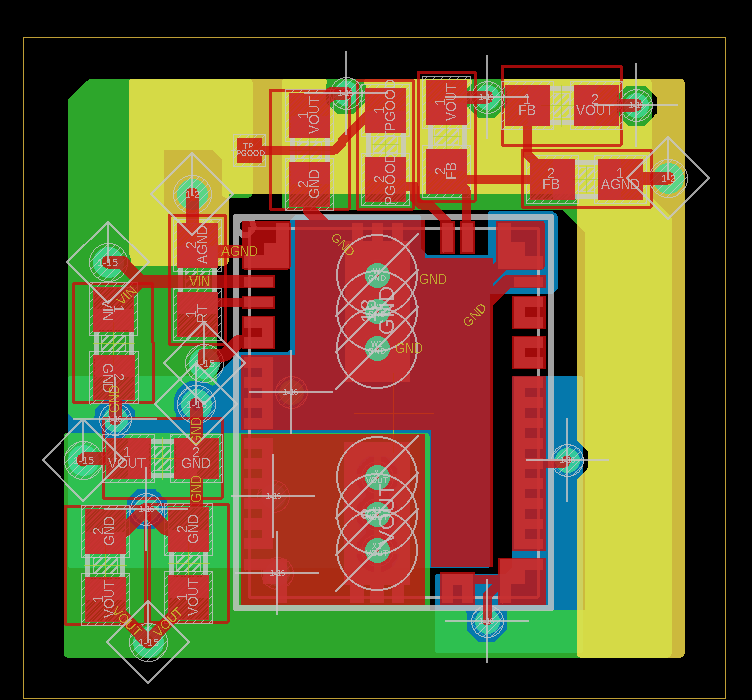
I'm using this lmzm module in the smallest possible PCB size, with 0603 passives, configuring for 5 volts output at 3A max. I don't know much about the relationship between copper area and thermal performance in PCB's, but i'm concerned that by minimizing PCB area i'm going to run into thermal dissipation issues. For reference, i'm using 4 layers total (for ground and voltage planes, as the manual suggests). Assuming the power module will be used in an outdoor environment, about 41°C max with direct sunlight, and about 2.25 watts power dissipated  (according to typical characteristics section of the data sheet).

How would I go about validating PCB area for this application while still keeping the PCB area to a minimum? I looked at the evaluation module for this power IC and it's much larger than what i'm using, but also has some modular abilities. I'm going for a minimalist, fixed frequency and output voltage approach.

  • Hi Andrew,

    Figure 42 in the datasheet should help guide you in PCB design with thermals in mind. It is good that you are using a  4 layer design since this will

    lower the expected thermal resistance(thetaJA) and allow more thermal relief than 2 layer boards.

    In your application of 2.25W and following the figure 42, if you designed the PCB area to be say 20cm^2 then you would expect to see the PCB heat up to 2.25W*(~22degC/W) = 50degC above the ambient temperature. As you increase the PCB area the PCB will heat up less. Since the device is rated with an absolute maximum IC junction temperature rating of 125C, you will be fine as long as the PCB temperature + ambient temperature is below the maximum value.

    Let me also refer you to a recently released app note that provide step by step procedure on how to determine your PCB area size. This should help you get started with PCB area layout considerations.

    Regards,

    Jimmy