


Other Parts Discussed in Thread: UC1708
Hi Team,
I received the following request. Can you help?
##############################
We are nowadays testing the UC1708-SP but we have trouble about it. If you can help on this IC, we can provide you our problem with details.
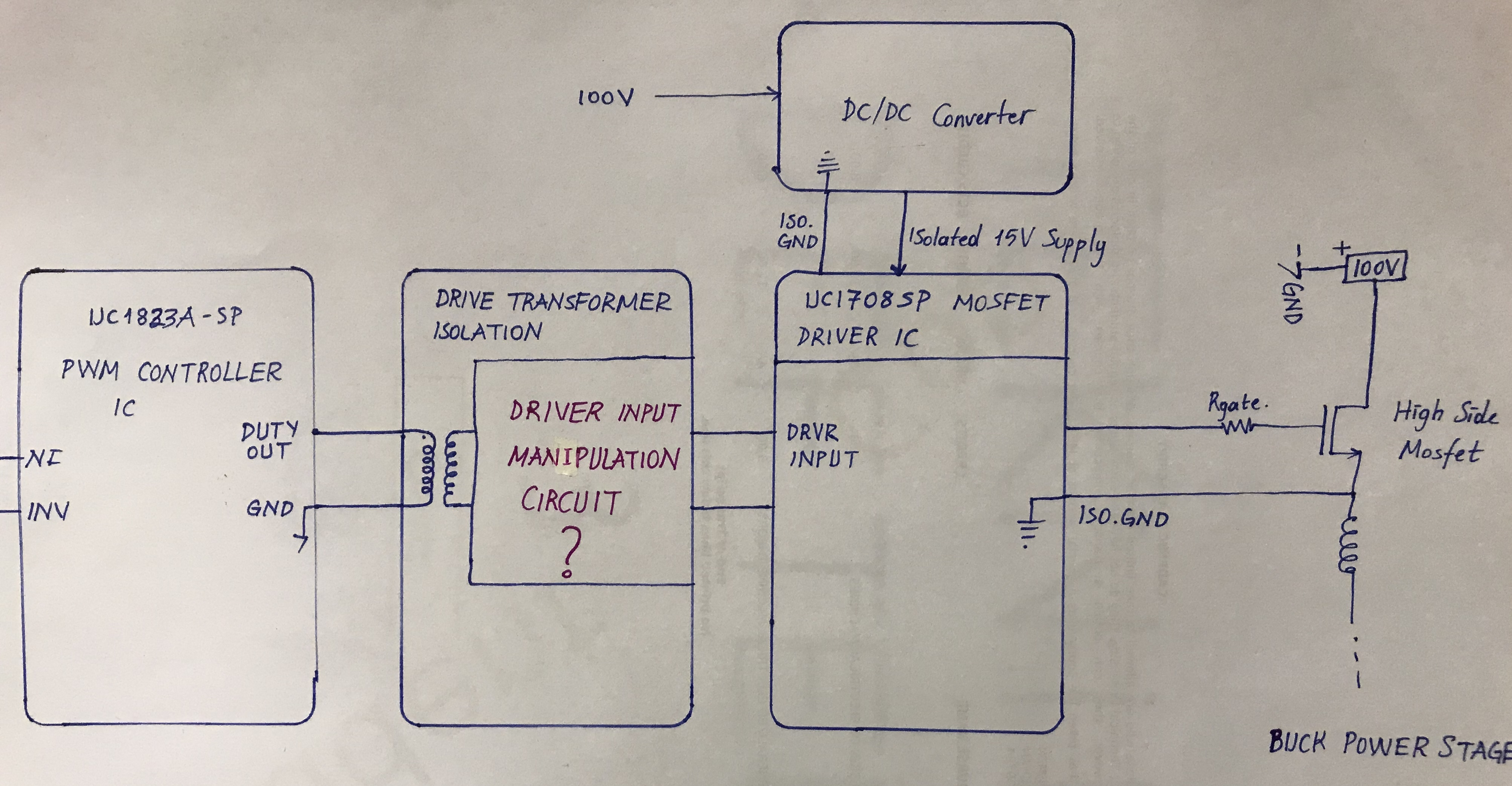
For brief explanation, we designed buck converter and we have high side NMOS. We supply UC1708-SP by isolated DC-DC converter. Therefore, UC1708 can drive high side MOSFET.
We send drive signals to IN pin with isolated gate drive transformer.
However, the IN pin characteristic is really interesting. UN1708 IN pin behaves like a voltage divider from its supply and some capacitance inside.
We also couldn't understand ENABLE pin characteristic.
The block diagram in datasheet is insufficient to understand the input characteristic.
If there is application note,design guide, it will be helpful.
Here the block diagram of our system. Our system requires high duty cycle.
We couldn’t understand the exact characteristics of DRVR INPUT pin of UC1708-SP.
We need stable interface circuit between pulse transformer and DRVR INPUT.
##############################
Regards,
Fabio
