Hello TI,
We have fev defects with this IC, TPS chip was latched-up when output has 0V or 4V (4V is correct value for our circuit) or 6V. In all case TPS IC don't respond for enable pin On/Off state (3.3V in our case). this defects was happened at multiple devices. problem dissapear after VIN reconnect. At some sets problem was happened again other sets works fine till now.
below oscilloscope screenshots with this problem in two cases, third one (0V lathed-up) i can't cath now.
6V output case:
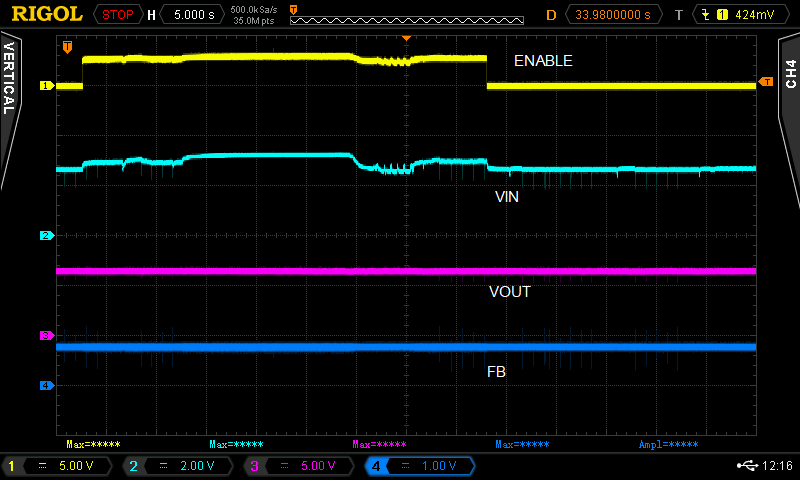
VOUT = 6.1 V
FB = 0.7V and it's not correct for this circuit.
VIN is floating in this case because this set battery was a little bit discharged what was effect of long time overvoltage at VOUT.
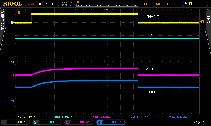
4V output case:
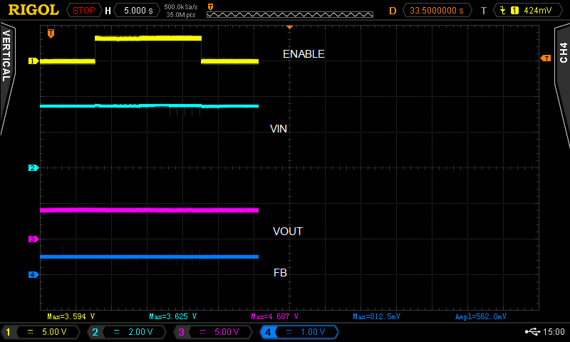
VIN: 3.6V
VOUT= 4V
FB=0.5V
Short explanation about our device:
Main supply - Lithium battery 3.6V and TPS63020 chip was supplied directly from this source, impossible to reconnect VIN in final device.
TPS63020 Vout = 4V and this is use for GSM module
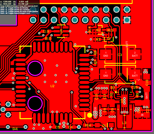
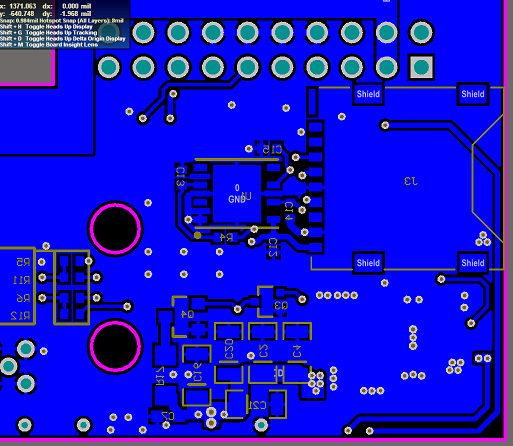
and part of circuit diagram:
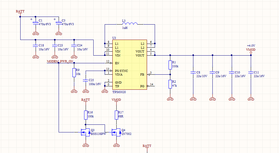
Q3 and Q4 are use for discharge VMOD after EN=off.