This thread has been locked.

If you have a related question, please click the "Ask a related question" button in the top right corner. The newly created question will be automatically linked to this question.

ISO5452: Isolated Gate Drive Design.

Part Number: ISO5452

Hello friends,

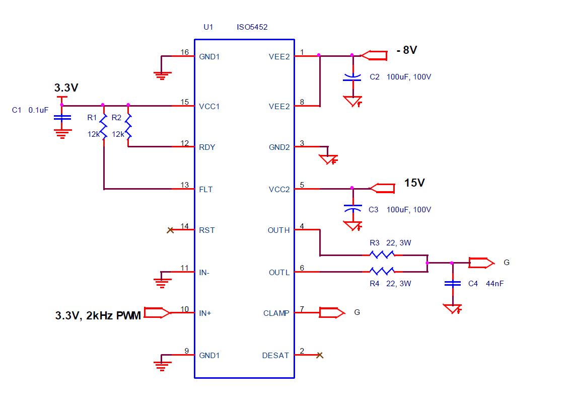
I am trying to test ISO5452 by mounting on general purpose PCB. I want to test it without IGBT by connecting a load capacitor across the OUTH/OUTL. The value of load capacitor is equal to the input capacitance of the IGBT. I have attached the schematic as shown below. The pin marked by cross is kept floating in our application.

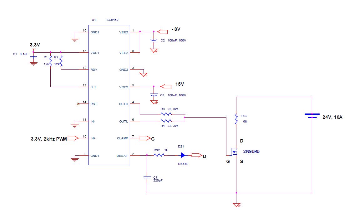
I want to check desat protection by connecting the recommended protection circuit (mentioned in datasheet) along with a load resistor. Please comment on the possibility of checking desat protection by this procedure.

  • Hello Vedang,

    Yes, you can use the recommended circuit as shown in Fig. 55 of the datasheet.

    You can find the typical waveforms for DESAT in Fig. 46. In order to test these specs you can use an AFG or voltage source at the DESAT pin referenced to GND2. Firstly, you can measure the actual V(DESAT) threshold by increasing the voltage at DESAT from 8V to 10V at 1ms increments. While doing this, monitor nFLT to determine what actual threshold voltage will trigger the fault. Next, you can find the delay from DESAT detection to OUTH/L, tDS, by gradually increasing the voltage at DESAT pin up to V(DESAT) which you measured. Then, measure the OUTH/L pin to see STO is activated. In both tests, IN+ should be held high at 3.3V.

    Please reach out if you have other questions.

    Regards,
    Audrey
  • Thanks. I will check the performance by above mentioned procedure and then revert back.
  • Dear Audrey,

    I have tested the ISO5452 along with MOSFET. The schematic is shown below:-

    During normal switching operation along with R32 resistor in the circuit, the voltage at the desat pin is -7.9932V with respect to source of mosfet. Also during short circuit (by bypassing R32 resistor) the voltage at the desat pin is -7.9V with respect to source of mosfet.

    Actually the voltage at desat pin as per datasheet should be between 8.3 to 9.5V. However I am having negative value and also the short circuit detection is not working.

    The desat diode used is BY203-12S. Kindly comment on the same.

    Regards,

    Vedang

  • Hello Vedang,

    That is unusual. According to your diagram, the DESAT circuitry does look correct. Could you please attach waveform image of your measurement of the Gate voltage with reference to Source and voltage at DESAT referenced to Source?

    Regards,
    Audrey
  • Dear Audrey,

    It was a mistake from my end. Connection problem was observed as a result of which DESAT showed improper voltage.

    However after changing the connection, I have observed the following results:-

    In both the images channel 1 & 2 corresponds to output PWM and Desat pin respectively. I have attached 2 images - normal and short circuit condition.I am not able to discern between time of short circuit to PWM shutdown. Kindly guide me so as to check the overall protection time.

    If you have any procedure for short circuit protection then please specify.

    Thanks & Regards,

    Vedang

  • Dear Audrey,

    I also want the design equation for changing the threshold for trigerring desat pin i.e, by changing number of desat diode, series resistor, zener diode, etc.

    Thanks & Regards,
    Vedang
  • Hi Vedang,

    In the first image, it looks like the DESAT pin has a large spike on it at the same time that the output turns on, then, as expected, the output falls and the device stops the output from turning on. In order to understand the timing better, you’ll need to zoom in to a much shorter time scale. The soft turnoff function should lower the output in ~2us, so you should use a comparable time scale when probing for this function.

    Please see this thread for more information on how to tune the DESAT threshold.

    https://e2e.ti.com/support/power-management/f/196/p/796343/2946036

    If this helped answer your question, could you please press the green button? If not, feel free to follow up.

    Thanks,

    John

  • Dear John,

    I am actually using IGBT (SKM300GB17E4) and the associated output characteristics of the same is shown below:-

    I am actually planning to provide the Desat protection at 4 to 5V as per the output characteristics. And so as per your previous reply, I will alter the desat protection circuitry.

    Please comment on the noise performance and also response time of desat pin for 4 to 5V threshold.

    Basically I am concerned about the nuisance tripping. 

    Thanks & Regards,

    Vedang

  • Hi Vedang,

    Based on the output characteristics of the device which you've shown, a DESAT threshold of 4V-5V should be suitable, although a higher voltage may also be acceptable for your chosen VGE of 15V. The response time of the DESAT pin from trigger to 90% OUTH/L is as specified in the datasheet, which is typically 553ns. Additionally, the glitch filter on the DESAT pin is 330ns.

    The blanking time, however, will change based on V_DESAT: t_BLK = (C_BLK*V_DESAT)/I_CHG; where I_CHG is 0.5mA, V_DESAT is 4-5V and C_BLK is the blanking capacitor. The blanking time t_BLK prevents false trigger and should not be smaller than the total turn-on transition from VGE(-) to VGE(+).

    Regards,
    Audrey
  • Dear Audrey,

    Thanks for your comment. So as per your comment I have summed up the calculation as shown below:-

    Response time of Desat pin = 0.553 microsecond.
    Glitch filter = 0.33 microsecond.
    Blanking time = 2.2 microsecond ( C = 220pF, V_DESAT = 5V).

    So total time turns out to be = 3.083 microsecond.

    Thanks & Regards,
    Vedang