This thread has been locked.

If you have a related question, please click the "Ask a related question" button in the top right corner. The newly created question will be automatically linked to this question.

TPS65261: Two TPS65261 cascades to power up the AM5706

Part Number: TPS65261
Other Parts Discussed in Thread: AM5706, , TPS51200

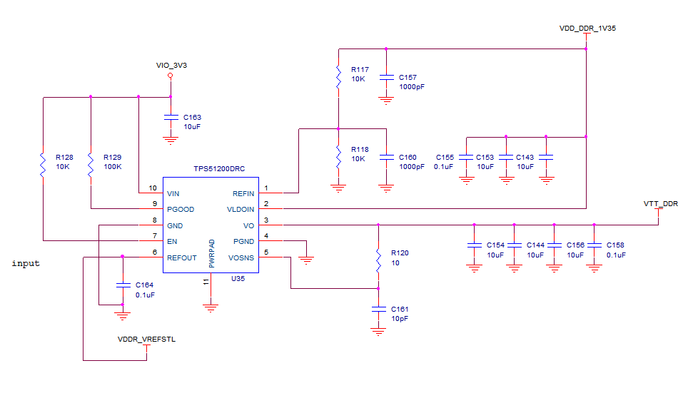
I want to use two TPS65261 cascades to power the AM5706. the VDDSHV_1 to VDDSHV_11  are all 3.3V.The power-up sequence I want to achieve is VDDS_1V8-----VDA_PLL_1V8----VDD_DDR_1V35 -----VDD_CORE_AVS-----VDD_DSP_AVS---VDA_PHY_1V8-----VIO_3V3.The attachment is the power circuit I have drawn. Is there a problem with this, why?1460.power.pdf

  • Hi, Sir

    Some comments:

    1. For U2 and U55, suggest to change input cap(C2 and C576) to 22uF MLCC, after that, place 22uF + 0.1uF input cap close to PVIN2/3 pin in layout, and place 10uF + 0.1uF input cap close to PVIN1 and VIN pin in layout.

    2. For BUCK1 of U2, the divider resisor is wrong, if its output is 1.8V, change R10 to 10kohm.

    Others look good.

  • First,In U55,can PGOOD1 only control EN1 to realize the sequence  VDD_CORE_AVS then  VDD_DSP_AVS THEN  VDA_PHY_1V8,OR NOT,PGOOD1 SHOULD  MUST CONTROL EN1 AND EN2 AND  EN3.

    Second,about the  ddr1_vref0. I use VIO_3V3 to produce ddr1_vref0 as pic below, Because the VIO_3V3 is the last power for AM5706,So i think the VDDR_VREFSTL(ddr1_vref0) is  too later away from VDDS_DDR1? Even i doubt it (ddr1_vref0)may after porz. Is my idea correct? Is there any good advice about this ddr1_vref0 power supply?

  • Hi, Sir

    Additional comments:

    For U2, the EN1/2/3 pin have internal pull-up current, so they can be floating, which means R455, R453, R451, R456, R454, R452, C584, C585, C586 can be removed.

    First,In U55,can PGOOD1 only control EN1 to realize the sequence  VDD_CORE_AVS then  VDD_DSP_AVS THEN  VDA_PHY_1V8,OR NOT,PGOOD1 SHOULD  MUST CONTROL EN1 AND EN2 AND  EN3.

    [Zhao] Actually, PGOOD1 only controls EN3 will realize your sequence, the EN1/2 pin can be floating too, and R457, R458, R459, R460, C588, C589 can be removed.  see below figure.

    Second,about the  ddr1_vref0. I use VIO_3V3 to produce ddr1_vref0 as pic below, Because the VIO_3V3 is the last power for AM5706,So i think the VDDR_VREFSTL(ddr1_vref0) is  too later away from VDDS_DDR1? Even i doubt it (ddr1_vref0)may after porz. Is my idea correct? Is there any good advice about this ddr1_vref0 power supply?

    [Zhao]

    When is the VDDS_DDR1 ready?

    What is the meaning of porz?

  • VDDS1_DDR1 is  the VOUT3(VDD_DDR_1V35) of  the  U2, porz is  just the H_PORZ which is the output of  U21, all of these power are in the pdf in the first question.

  • Hi, Sir

    1. I checked U21's datasheet, it looks have 300mSec delay, so i think ddr1_vref0 will not after porz.

    2. The estimated delay time from VDD_DDR_1V35 to VIO_3V3 is ~7mSec. I checked U35, it looks there is no delay from EN to ddr1_vref0.

    Can it be accepted in application?

    But for TPS51200, i am not sure if it is allowed VIO_3V3 comes after VDD_DDR_1V35.  

    BTW, i am not in charge of TPS51200, please send mail to me and i will forward your questions to relevant engineer.

    zhao-ma@ti.com