This thread has been locked.

If you have a related question, please click the "Ask a related question" button in the top right corner. The newly created question will be automatically linked to this question.

BQ76940: TIDA-010074 schematic query

Part Number: BQ76940
Other Parts Discussed in Thread: TIDA-010074

Hi

I have some queries about TIDA-010074

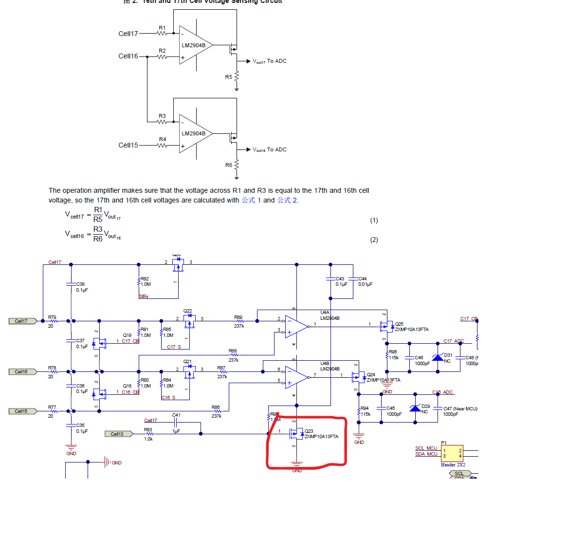
1. VDD of the op amp is CELL17+, VSS is CELL13+, and a 1M resistance between VSS and CELL13+ will not affect the power supply?What does Q23 do in the schematic diagram?Seems to be off all the time?

2. As shown in the figure, what is the function of P MOS? This connection seems to be different from the usual op amp output to the v-end; How did this formula come out? Vcell16 = R3 / R6 * Vout16

Waiting for your repoy

Thanks

Star

  • Hi Star,

    This is new reference design and I will loop in the expert who created this circuit. He is out of office today, but will be able to reply on Monday.

    Sorry for the delay,

    Matt

  • Hi Star,

    1. The 1M R90 will bias the negative supply of the op amp to the filtered cell 13 voltage if the amp draws no current.  When the amp draws sufficient current to create the Vgsth voltage of Q23 across R90, Q23 will conduct and the remaining current for the op amp supply will flow through Q23 to GND.  So the majority of the current for the amp is across all cells with only a few uA across cells 14-17.  

    2. The P-ch FET at the amp output is to keep the amp output current out of the measurement result. The basic description of the voltage-to-current converter circuit is in the TIDA-010074 design guide http://www.ti.com/lit/ug/tidues4/tidues4.pdf section 2.3.1. Consider the cell 16 amplifier and figure 2 of the design guide.  The op-amp is considered ideal, so no current flows through R4 into the positive input and the positive input is the cell 15 voltage.  The op amp will adjust the output to make the inputs match, so the voltage across R3 is the cell 16 voltage (Vcell16-Vcell15).  The current in R3 is CELL16/R3.  With the P-ch FET at the amp output, no current flows from the gate to source or drain steady state.  There is no current into the inverting input of the amp, so all current through R3 must go through the P-ch FET and through R6.  The output voltage across R6 is IxR or Cell16/R3 x R6 or Cell16 x R6/R3 = Vout.  The MCU will get the Vout, to convert back to the cell voltage multiply by the inverse of the resistor ratio which is equation 2.  Of course the Q21 switch is not zero current: there will be some drop across R78 from the switch current and the measurement current, the resistors have tolerance, and the amp is not ideal, so as the design guide states some correction trimming will be needed for the voltage sensing accuracy.