This thread has been locked.

If you have a related question, please click the "Ask a related question" button in the top right corner. The newly created question will be automatically linked to this question.

TPS548A20: Schematic Review for 12V to 3.3V 10A

Part Number: TPS548A20

Hi TI expert,

Could you help to review the schematic with TPS548A20? Do we need to consider to add heatsink since we need to support 70°C?

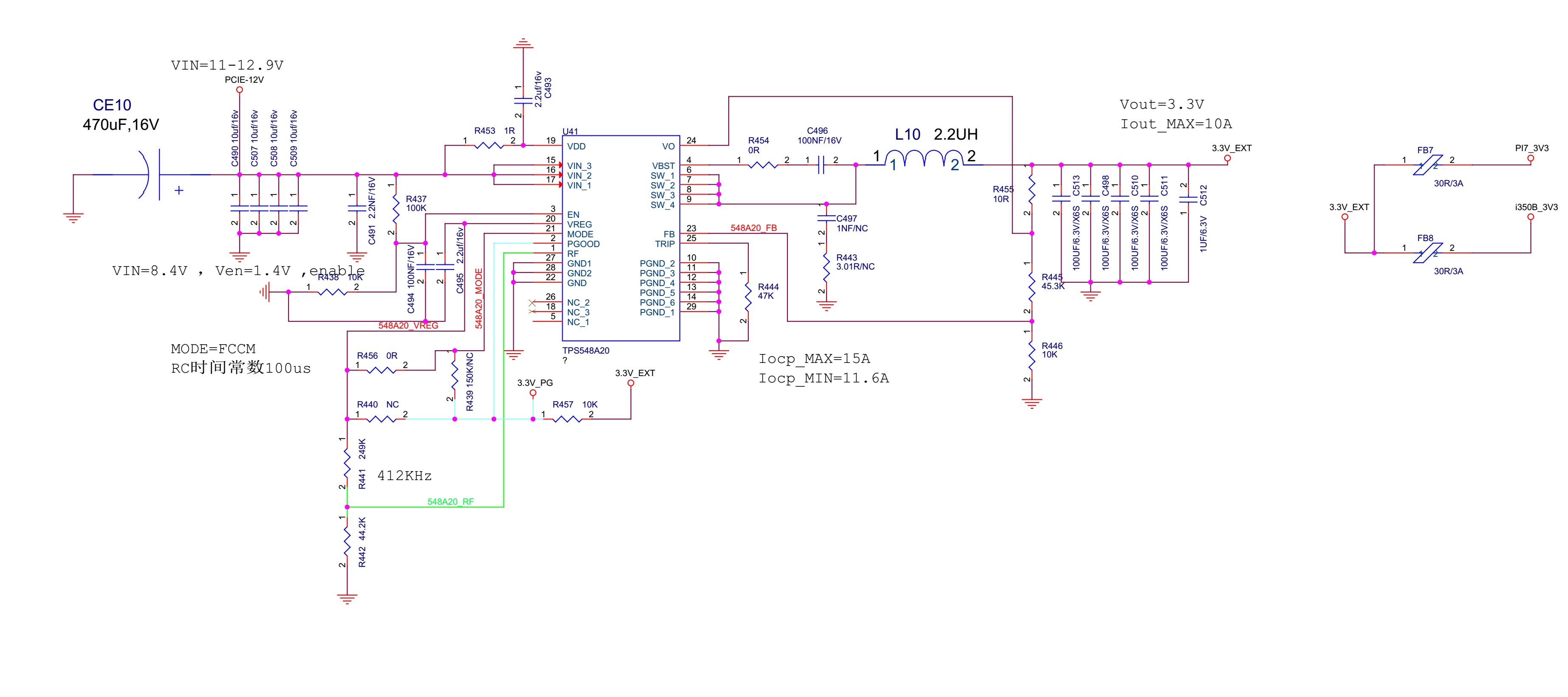
Vin: 12V (11V~12.9V)

Vout: 3.3V

Iout: 10A max (5A for the thermal and power loss consideration)

Operational Ambient: -10°C to 70°C

PCB layers: 10 layers. 

Some questions:

1. Do we need to consider to add heatsink since we need to support 70°C? The webench simulation result seems too good on efficiency, comparing a test result with 12V to 1V 15A 500Khz. 

2. Do we need to do bode plot test for such DCAP3 control? Will our design be stable? Per the datasheet, the LC pole and a zero are mentioned. But no much idea how to calculate the phase margin and cross-over frequency with the selected components.

 Thanks,

Dora

  • Dora, 

    I am reviewing your schematic. 

    I will summarize and post on 9/13/2019

    Regards,

    David

  • Hi Dora,

      The TPS548A20 has an absolute maximum junction temperature of 150C. The operating ambient temperature is -40C to 125C ( as long as the junction temperature is not exceeded). The device does have a thermal pad to help with dissipating the heat, however the package does not support mounting an external heat sink. For 70C ambient, the device should be able to operate for your specification as you can see in the WEBENCH design, the Tj of the device is around 106degC - lower than the absolute Tj max of the device.

    Was this design created using WEBENCH? If so, that helps with schematic reviews very much. Can you please share the WEBENCH design?

    Regarding bode plot for DCAP3 devices, it is always to good to measure the loop response of your design to verify that you have enough gain and phase margin.

    Here is a blog post that gives you information on how these measurements could be done. http://e2e.ti.com/blogs_/b/powerhouse/archive/2017/05/24/comparing-bode-plots-in-d-cap3-control-mode

    Here is an appnote that talks about the loop model for DCAP2. We dont have an analytical loop model for DCAP3 at the moment. Measurement on the board is what we recommend.

    http://www.ti.com/lit/an/slva546/slva546.pdf

    Regards,

    Gerold

  • Hi Gerold,

    The design is based on Webench result, but not exactly the same as Webench. 

    It is adjusted a little bit based on the space limitation(for output inductor, output capacitor). And mode pin and PGOOD pin connection are different bacause we want to use 3.3V_PGOOD to enable another 1.0V DC/DC. 

    Attached the webench design as below. 

    tps548a20.pdf

  • Figure 1 to 4 on page 8 of TPS548A20 of datasheet graphs efficiencies at different output voltages.

    The 3.3V efficiency is similar to the calculated efficiency from Webench. 

    The  webench report you attached on page 3 shows Tj vs output current.

    At 5A, the Tj is 97.5C and at 10A output current the Tj is 122.5C which are lower

    than the recommended operating temperature.   

    Follow the layout recommendations regarding thermal vias to achieve similar results. 

    Some designers use the spice models to estimate the stability. 

    TPS548A20 PSpice Transient Model

    www.ti.com/.../slum498

    David