This thread has been locked.

If you have a related question, please click the "Ask a related question" button in the top right corner. The newly created question will be automatically linked to this question.

TPS548D21: Via requirement for Thermal pad

Part Number: TPS548D21

Hi,

We have designed a board using the TPS548D21 regulator. The current requirement in our design is 26A.

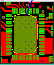
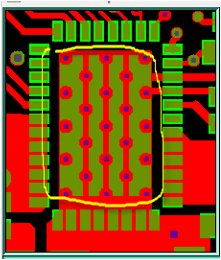
Under the thermal pad, we have provided 23 Vias of 18mil pad diameter and 8 mill drill size.

These via pads are masked and plugged with solder mask ink, and not filling the via to avoid assembly issue(Solder paste ingress into via barrel).

Hence, the thermal pad contact area to the PCB has been reduced, please refer the attached image yellow circled area.

The query is, whether increasing the via count further will improve the thermal performance of the regulator?

Regards,

Magesh.M

  • Hi Magesh,   

                     Are you mentioning that the vias are isolated and not connecting electrically to the copper area on the thermal pad?

    In general increasing the thermal vias, would help increase the surface area available for the heat to be dissipated and hence improve the thermal performance. This is because there is connectivity between the copper in the thermal pad and the vias.

    Regards,

    Gerold

  • Hi Gerold,

    The vias are physically not touching to the regulator thermal pad as they are covered with solder mask ink. But, on PCB level, they are electrically connected to the copper shape of footprint's thermal pad.

    We plan to increase the via count and open solder mask for via to improve the thermal contact area as shown below. Via count increased from 23 to 33.

    Is there any quantitative thermal data available,

    1) For increased via count

    2) For Increased Surface contact area

    This will be useful for comparing/making decision on thermal improvement.

    Regards,

    Magesh.M

  • Magesh,

    Since the TPS548D21 uses the PCB ground copper as the primary heat dissipation path to ambient, improvements to the thermal path from the primary heat generator - the low-side FET which is soldered directly to the interior of the thermal pad - and the PCB ground plans will improve the thermal performance.

    A 1-oz plated weight via on an 8-mil drilled hole has about 80 degrees C/W thermal resistance.

    3.47 C/W for 23

    2.42 C/W for 33

    Increasing the solder coverage area also likely reduces the thermal path about 1C/W.

    The reduces thermal resistance to the copper plane also improves the Copper plane to Ambient thermal dissipation as it increases the effective area of the PCB that is hot enough to  dissipate heat.  The net effect of all three would be a 3-4 degrees C/W reduction in the thermal path from the IC die to the ambient are and a corresponding reduction in the IC die temperature.

  • Hi Peter,

    Thanks for the data provided. This addresses my query.