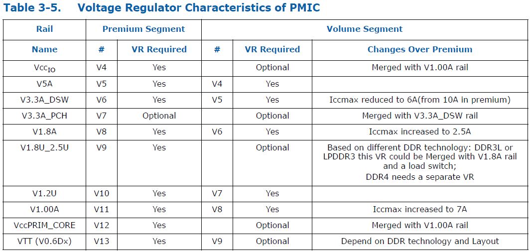
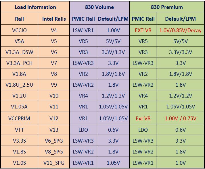
Data sheet SLVSCF4A DECEMBER 2014 Table 6-57 refers to NODES V4, V5, V6, V7, V8, V9, V10, V13.
These nodes should be regulator outputs, but I can not see where in the document these nodes are defined. A simillar problem exists for Table 6-63. Where can I find the definition of these nodes?