This thread has been locked.

If you have a related question, please click the "Ask a related question" button in the top right corner. The newly created question will be automatically linked to this question.

TPS63802: Output ripple voltage is almost 2 Vpp

Part Number: TPS63802

Hello,

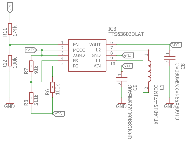
I am using TPS63802 for my Low power device with BLE113 module. I need to power that from Li-ion. So I chose this circuit for stable 3.3V output.

For circuit I used WEBENCH, so all my values corresponds to WEBENCH tool.

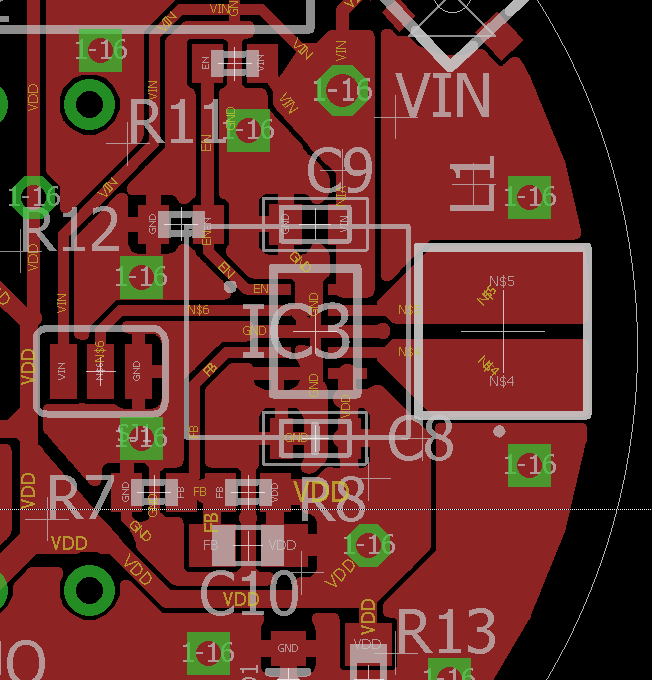
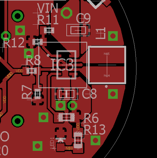
My PCB layout is also similar to EVM board

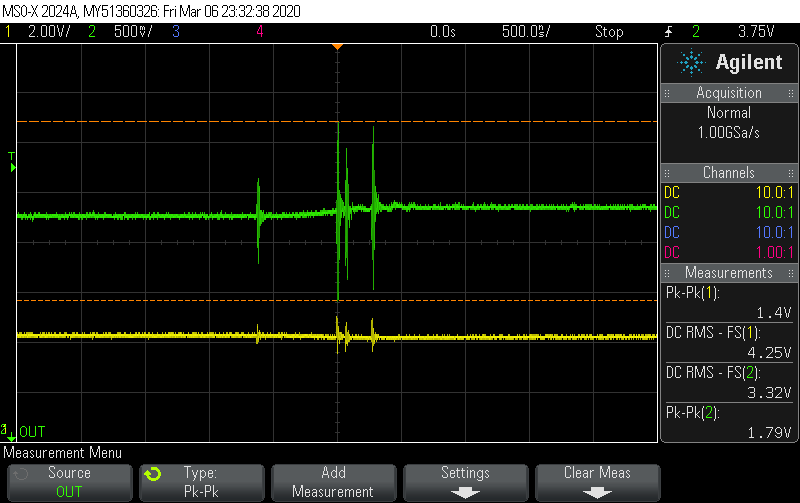
And when I connects the power, the input voltage (Yellow) and the output voltage (green) is shown on my scope as overall signal

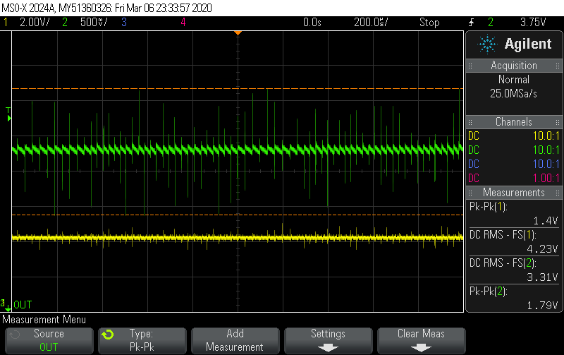
I tried to change input voltages from all the range (4.2V - 3.0V) and I always see the spikes. The zoom of that spikes is on next image.

I tried to add 100nF capacitor on the output close to TPS IC. I tried to use several feedforward capacitor ranging from 1pF to 100pF paralel to my R8 resistor (from output to FB pin).

I found in datasheet of BLE113, that it allows voltage ripple less than 10mV. And I don't know how to smooth the output voltage.

Do you have any suggestion please?

Regards

dbarvik

  • Hi dbarvik,

    The spikes you see might just be noise your scope probe is picking up. Make sure you are measuring the ripple properly, these articles might help you:
    https://e2e.ti.com/blogs_/b/powerhouse/archive/2016/07/27/how-you-measure-your-ripple-can-make-you-or-break-you
    http://www.ti.com/lit/an/slva494a/slva494a.pdf

    From what I can see in your scope images is that the ripple is around 100 mVpp (if you were to remove the spikes from the green trace, or turn on 20-MHz filter), which is typical for Vin = 4.2 V, Vout = 3.3 V in power-save mode. If this is still to much you need to operate the device in forced-PWM mode by connecting MODE pin to VIN. The ripple is then around 10 mVpp, but the efficiency at low currents will be lower. This is a compromise between the efficiency at low currents and the output ripple. You can also dynamically change the operating mode by toggling the MODE pin to switch to forced-PWM mode when low ripple is important and to power-save mode when the circuit is in standby.

    I also have a few remarks for your layout:

    1. Move C9 closer to the device and make sure the GND return from C9 to PGND of the TPS63802 is in the top layer and as short as possible.
    2. The line from VOUT to high side of R8 should be as short as possible. I would move R8 and place it just after C8.
    3. If you are not using PG pin, you can remove R6 and leave PG pin floating or connect it to GND.

    Points 1 and 2 are very important, if not properly done, they can increase the noise and destabilize the device. Here are some application note on how to do a good PCB layout when using switching converters:
    http://www.ti.com/lit/an/slva773/slva773.pdf
    http://www.ti.com/lit/an/slyt614/slyt614.pdf

    Best regards,
    Milos 

  • Hello,

    thank you for the reply, I tried to redesign my PCB. Could you please check it, if it is correct now? 

    Thank you.

    Regards

    dbarvik

  • Hi dbarvik,

    The layout looks fine to me, much better than the previous version.

    Did you try to take new ripple measurements?

    Best regards,
    Milos

  • Hello

    thank you, and yes, I was wrong with the ripple measurement, I measure thin peaks in the signal, not the ripple.

    The ripple is now 50 mV and this is much better previous measurement.

    Regards

    dbarvik

  • Hi,

    Great. Then I will close this thread. If you have any other questions you can come back here, or open a new thread if this one get locked after some time.

    Best regards,
    Milos