This thread has been locked.

If you have a related question, please click the "Ask a related question" button in the top right corner. The newly created question will be automatically linked to this question.

TPS53219A: TPS53219A's DC offset vs EVM test

Part Number: TPS53219A

Hi Team,

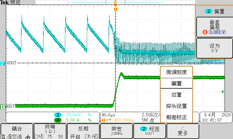
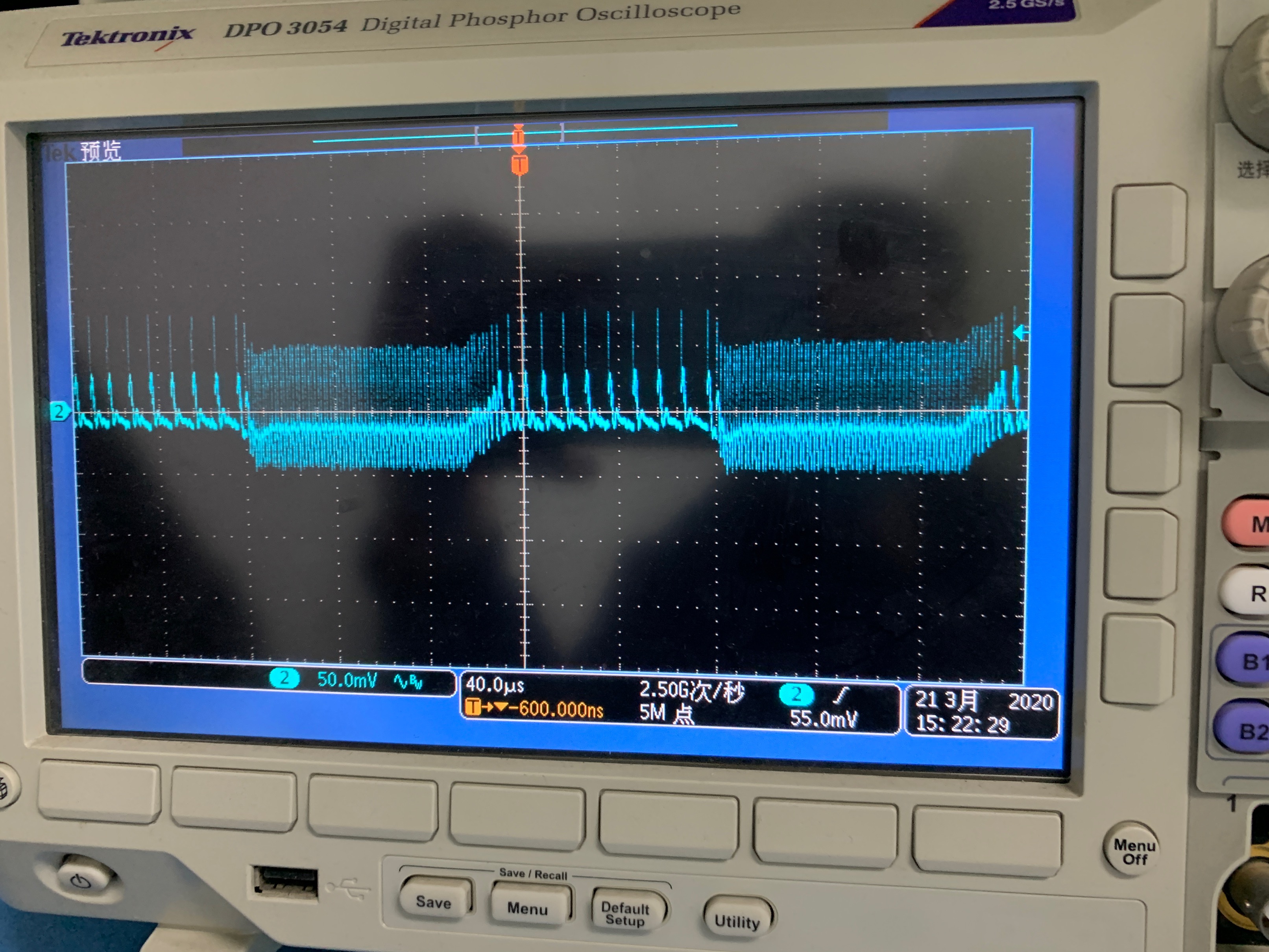
While I was testing TPS53219A's EVM output ripple with the ripple injection cap removed (true DCAP1), the result below. There is an approximately 20mV DC offset between light load and heavy load. It is very strange as DCAP1 should not have any DC offset.

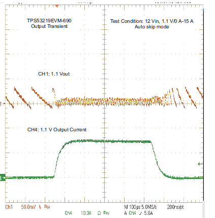
After that, when I turned to EVM user guide, there is no offset though.

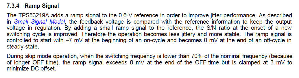
I know offset is led by ramp compensation on the reference. According to datasheet, ramp will generate DC offset, so this exists in any load condition. However, it is too strange that test in EVM does not show any DC offset. 

Could you please help me point out the reason?

-Wenhao

  •  

    The EVM is actually showing a DC offset shift between the no-load state and the loaded state as the ripple voltage increases under voltage light load conditions. 

    The oscilloscope which shows the valley voltage dropping under load is most likely a result of switch-edge noise from the switch edge.  If you look closely at the waveforms, the voltage is primarily (darkest band) at the same voltage as it is under the light load condition.  I would suggest changing the scope from AC coupling to DC coupling with an offset and looking at the output voltage at very light load and heavy load with a higher horizontal resolution, 5 or 10us per division, so you can see the difference between the switch edge noise coupling into the measurements and the ripple on VOUT.

  • Hi Peter,

    Thank you! That means a lot to the design. I will update the test and reply you soon.

    -Wenhao

  • Hi Peter,

    I did the experiments as your reference below. As you can see closely, I set the DC Offset of channel 2 to 1.081V, and DC coupling. From the valley side you can see there is no switching noise which triggers the onset. So it has to be an internal ramp exerted to Vref which makes output to have an offset. As this I am not able to replicate same waveform stated in EVM user guide. May you see the analysis and tell the reason? Thanks!

  •  

    I am not sure what you mean by "I am not able to replicate same waveform as in EVM users guide.  The only difference between your waveform above and figure 8 in the User's guide is the switching noise that the scope is picking up during continuous conduction, and the voltage scaling on the EVM figure 7 was taken at 50mV/division verse 20mV per division in the data you took.

    At near zero load, the output voltage rises up then decays very slowly with the low-side FET off and no inductor current.  When the FB voltage decays to the reference voltage plus the +3mV of ramp, a new on-time is started.  When as the load current increases, less of the inductor ripple current flows into the capacitor and the ripple current decreases.  As the load current exceeds have of the peak to peak ripple current, the inductor current becomes continuous, the ripple amplitude is about 1/4 of the no-load ripple current and the ramp reduces from +3mV to 0V, decreasing the valley voltage on the FB pin by about 3mV to the reference voltage.

    At that point, the increased current in the FETs during the switching increases the switch-noise picked up by the Oscilloscope and we see a wider noise band around the output voltage.  With a 0.6V reference and a 1.1V, the 3mV shift in the reference voltage results in about 6mV decrease on the output voltage.