This thread has been locked.

If you have a related question, please click the "Ask a related question" button in the top right corner. The newly created question will be automatically linked to this question.

CSD95373AQ5M: About VIA layout on recommended thermal pad

Part Number: CSD95373AQ5M

Hi,

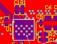
Could you tell me the recommended VIA layout dimensions on the thermal pad?


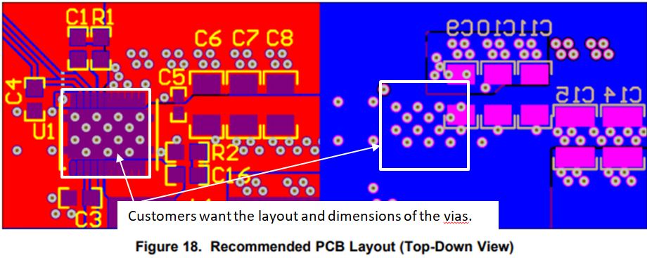
There was no description of the via size in the data sheet.
Customers want information similar to the following:
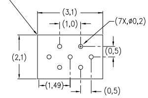


Regards,
Yusuke

  • Hi Yusuke,

    Unfortunately, we don't have a PCB drawing with vias for this part, but you can find the via size recommendations at section "9.1.4 Thermal Performance" on datasheet.

    Thanks!

    Best regards

    Bo Wang

  • Hi Wang,

    Thank you for your support.
    I will contact the customer with the following:
    >"9.1.4 Thermal Performance"

    However,
    If there is a layout example, there should be its dimensions and layout drawing.

    Could you provide the following layout design information?


    Regards,
    Yusuke

  • Hi Wang,

    Thank you for your kind support.
    Is there any update about Via layout information?

    Best regards,
    Yusuke

  • Hi Yusuke,

    This EVM is an old design, we used PADs for the design. We changed from PADs to Altium for PCB design several years ago and don't have the access to PADs anymore. I'm still checking to see if there is a way that I can get the information for you.

    Thanks!

    Best regards

    Bo

  • Hi Yusuke,

    Unfortunately we don't have a drawing for this part. But CSD95373 has similar package as CSD95490Q5M, probably you can use CSD95490 via placement on datasheet as reference:CSD95373 has a little larger GND pad than CSD95490, but  you can start with a GND via at the center of the GND thermal pad, then use the distance info to place the other vias,

    Thanks!

    Best regards

    Bo

  • Hi Bo,

    Thank you for your kind support.
    I received an additional question about VIA information from customer.
    Could you give me your advice?

    ・Is there an ideal aperture ratio for a metal mask opening relative to a pad?
     Or Is there a target value (xx%) for the bonding ratio between the thermal electrode and the pad on the board?

    Best regards,
    Yusuke

  • Hi Yusuke,

     Please see below for the answers:

    (1) Is there an ideal aperture ratio for a metal mask opening relative to a pad?

    To maintain good bond line thickness of solder it is recommended to target at least 65% coverage. However we may need to look at the complexity of the pads as we will be dealing with different area and sizes. But as default 65% coverage is good for solder voiding and BLT

    (2) Or Is there a target value (xx%) for the bonding ratio between the thermal electrode and the pad on the board? 

     >50% of the area is OK, <50% will impact the electrical and thermals


    Thanks!

    Best regards

    Bo