This thread has been locked.

If you have a related question, please click the "Ask a related question" button in the top right corner. The newly created question will be automatically linked to this question.

TPS61236P: The output can't reach the set value

Part Number: TPS61236P

Hi,

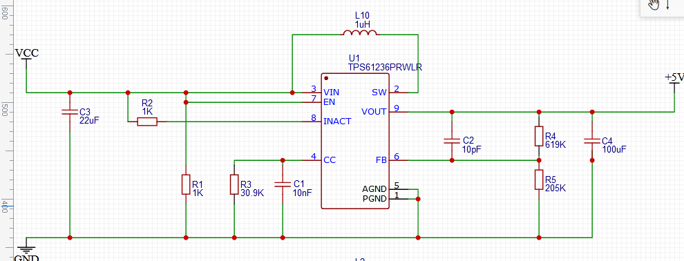
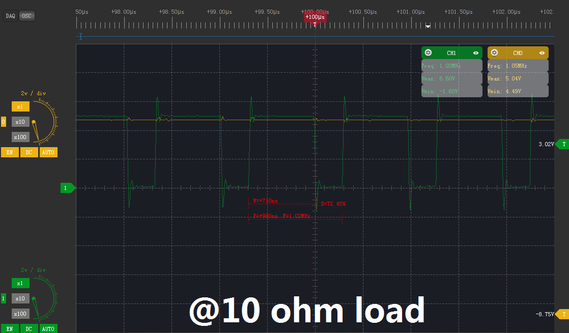
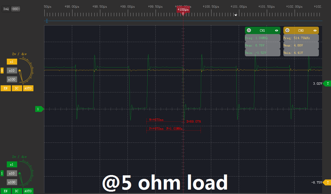
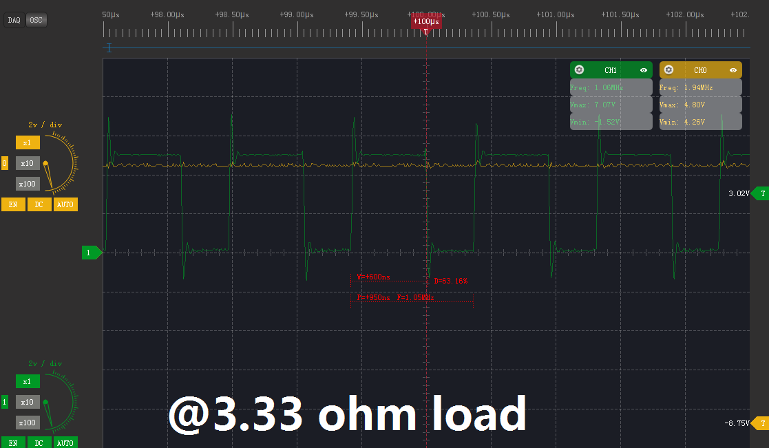
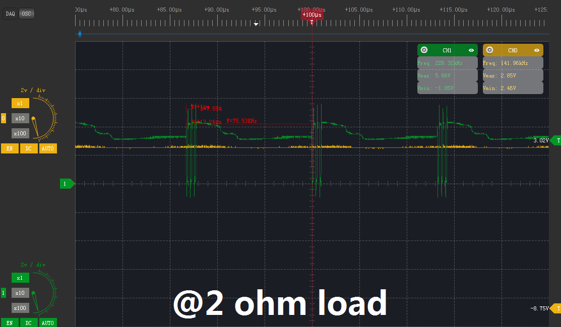
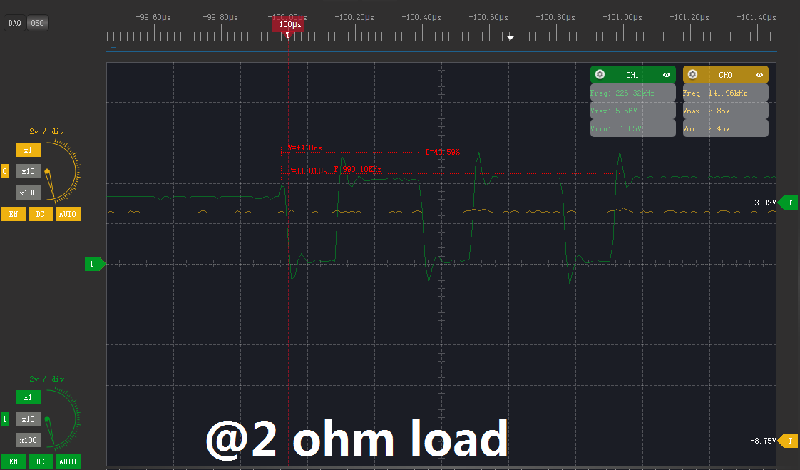
I have built a li-ion to 5V @ 4A constant current DC converter using TPS61236P (the circuit and most of the resistor and capacitor values come from WEBENCH while some changed a little) but it turned out that the output can't reach the set value. I connected a 3.33Ohm resistor as a load, and the current should be 1.5A, but the output current was around 1A and the voltage was around 3.3V ---- even lower than the 3.8V input!

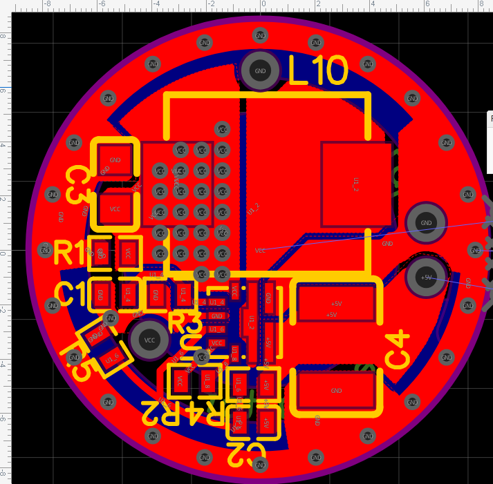
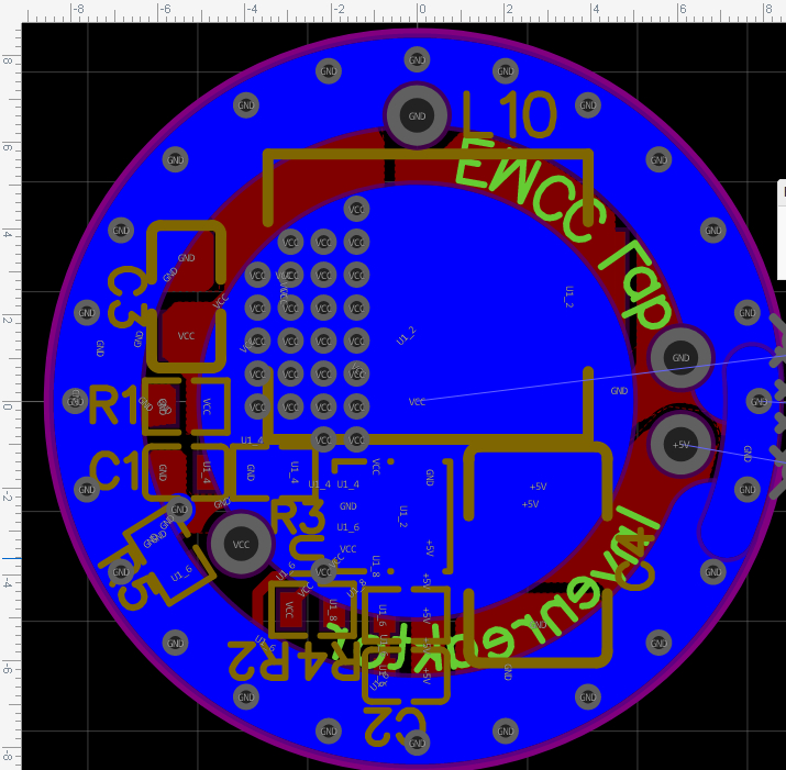
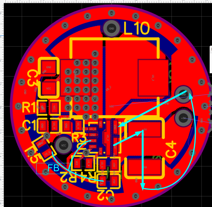
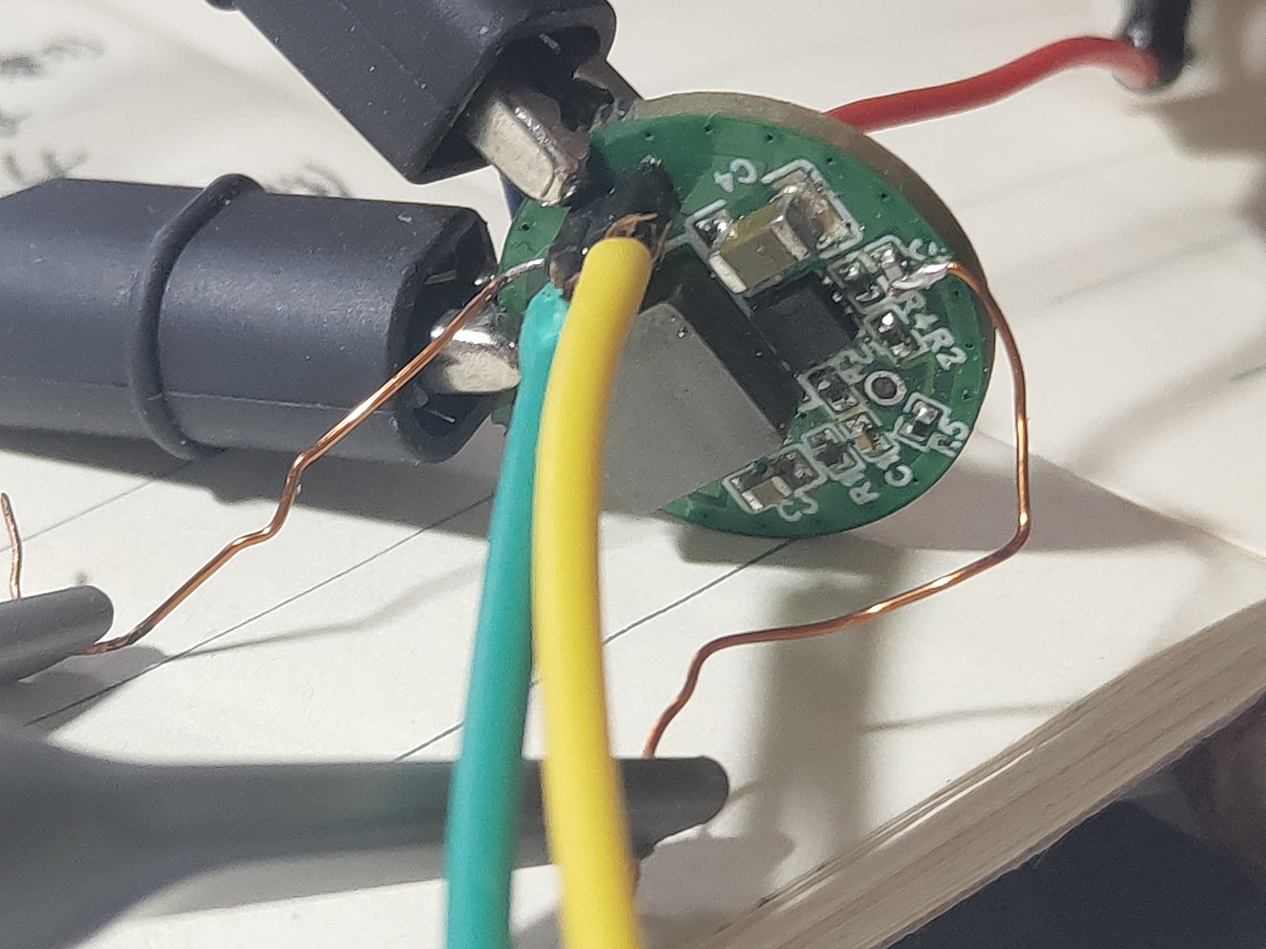
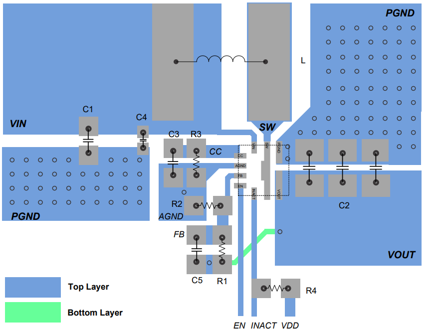
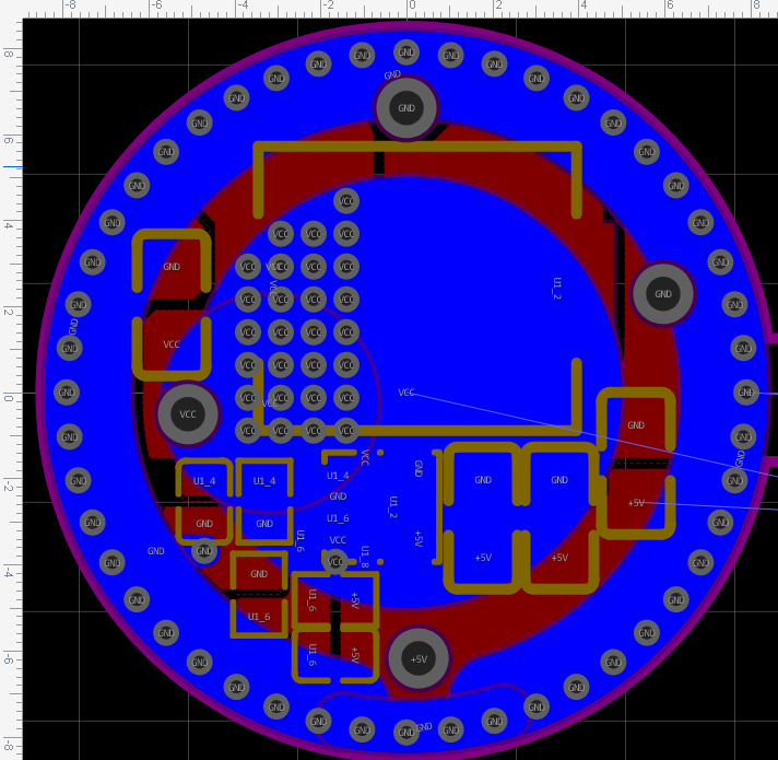
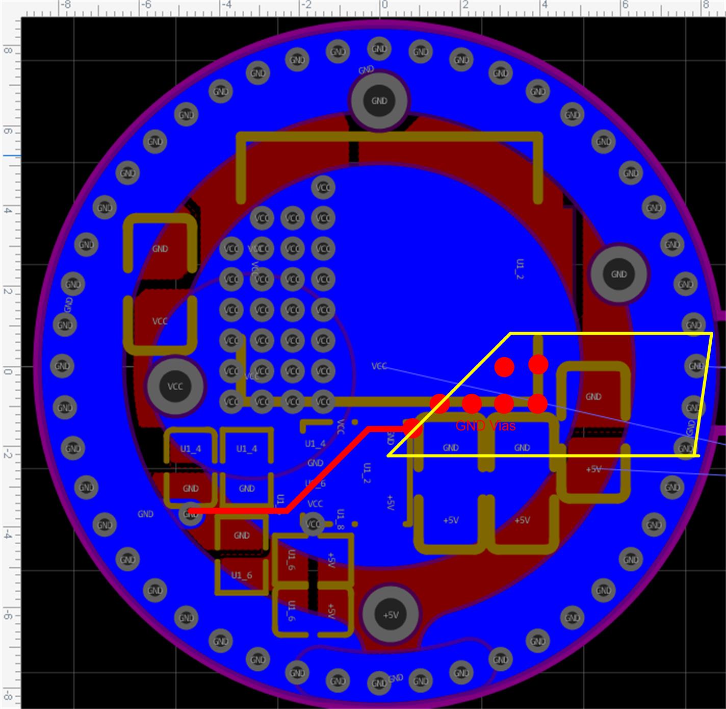
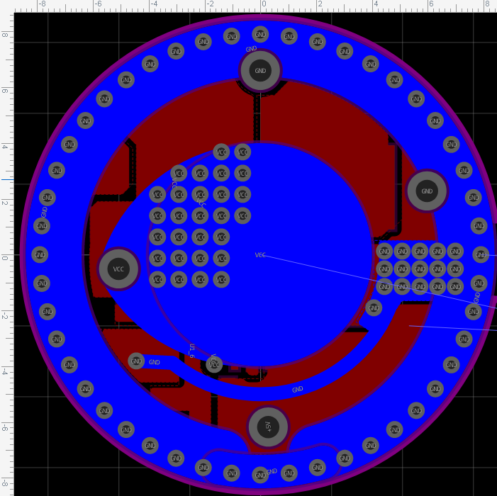
The schematic and both side of the layout are attached.

Thank you so much.

  • Hi,

    Have you tried applied the 3.3ohm resistor load after the Vout reaches 5V? It may triggers the pre-charger current limit during startup. That's why the Vout is clamped at low level.

    Besides that, the output capacitor C4 placement is not recommended. The IC GND pin is not connected to C4 GND pad directly.

  • Hi Zack Liu,

    Thank you so much for quick reply.

    I applied the 3.33ohm resistor load after the Vout did reach 5V really. Actually, I always apply load to the converter several seconds or longer after the converter is powered.

    As for the output capacitor C4, did you mean that three 22uF replaced by one 100uF is not recommended?

    As for the GND pad layout, I will fix it later.

    Thanks a lot.

  • By the way, the output behavior is same when I disable CC by shorting C1 & R3.

  • Hi,

    So you mean if no load the Vout is correct of 5V. When the 3.33 ohm is applied at output, the Vout drops to 3.3V?

    Please make sure the input 3.8V has enough current capability. For this case, the input current should be at least 5V*4A/3.8V/0.9=5.05A. 

    What's the part number of this 100uF capacitor? Usually paralleling three ceramic capacitors would have lower ESR and ESL, so the output voltage ripple would smaller. But this should not be the root cause of the output voltage drop. Please also let me know the part number of inductor. Thanks.

  • Hi Zack Liu,

    Zack Liu said:

    So you mean if no load the Vout is correct of 5V. When the 3.33 ohm is applied at output, the Vout drops to 3.3V?

    Yes, so as you said.

    As for the 3.8V power supply, whether it can output 5A has not been tested. But when I apply 3.33ohm to the converter, no significant voltage drop of 3.8V power supply was found. It seemed that its current capability is enough, but maybe only for the 3.33ohm load.

    The 100uF capacitor is made by TAIYO YUDEN and its part number is JMK316BJ107ML-T.

    The inductor is made by TDG (not TDK! ) and its part number is TMAX-0630-1R0-M.

    Thanks a lot.

  • Hi,

    For a boost converter, the output voltage is higher than input voltage so the input current needs to be higher than output current. In your case, like I said, the input power supply should have 5A capability. If you test it with a 3.33ohm, you only approve it can output 3.8V/3.33=1.14A. You can use a external power supply to test the board first.

    Secondly, the 100uF capacitor JMK316BJ107ML-T voltage rating is only 6.3V. By searching the capacitor datasheet, the effective capacitance is only (1-70%)*100uF=30uF. It's OK for this application. But ripple may be high. If possible, use three 10V voltage rating capacitors in parallel so that total effective capacitance is higher.

    The inductor is OK.

    If the Vout still drops when a 3.33ohm load is applied, can you probe the SW, Vout, Vin with digital oscilloscope and share the waveform. Thanks.

  • Hi,

    Is there any update?

  • Hi Zack Liu,

    I've got the waveforms of different loads, from 10 ohm to 2 ohm. The channel 1 is Vout and the channel 2 is the SW. At this time, things are a little different. When the load resistance is 3.33 ohm or higher, the waveforms were basically good, while the load was 2 ohm, Vout dropped to nearly 2.5V and the waveform became abnormal. The power supply had been replaced by a Li-ion battery which is used for drones before this test. It can output dozens of amps and I believe it's enough. The waveform are attached below.

    Thanks a lot.

  • Errata:

    user6294971 said:

     The channel 1 is Vout and the channel 2 is the SW.

    The channel 0 is Vout and the channel 1 is the SW. By the way, the parts of the circuit had not been changed, including C4.

  • Hi,

    Thanks for sharing the test waveform.

    The main reason would be the output capacitor layout, like I said in the first reply one week ago.

    The test waveform shows the device would work with no issue at low load current condition.But when load current is high, during switching, the output capacitor charging path is too long shown in below picture. The current will flow through Vout pin, Cout C4, and back to GND pin through a very long trace. This will introduce a big PCB parasitic inductance and cause device works abnormally. Thus, the feedback network R4, R5, C2 placement is not good. These components should be placed close to IC with short trace because FB pin is very sensitive to noise. 

  • Hi Zack Liu,

    To verify whether the FB pin is really interfered, I've probed the waveform of SW & FB. It's not very easy to connect to the oscilloscope so I soldered copper wire to the FB net (as the photo shows below), but this may enhance the interfering. What's more, since the input resistance of my oscilloscope is not so big, when the oscilloscope was connected, Vout rose to 5.73V.

     Because there are too many waveform screenshots, I zipped them instead of uploading them directly. But it seemed that FB was really interfered.

    fb@3.33ohm.zip

  • Hi,

    Thanks for sharing the waveform and test result.

    Yes, The FB is always very important for a high frequency switching power supply. That's why this device keeps a analog GND (AGND) pin in order to keeps the feedback trace clean.

    In your layout, the AGND connecting to PGND trace is long. And the output capacitor charging and discharging current will also flow through the same trace. 

    See below recommended layout and EVM user's guide link. The AGND is connected to PGND through inner layer so that FB signal is not interfered by switching current and noise. 

    https://www.ti.com/lit/ug/slvuad0a/slvuad0a.pdf?ts=1588128039998

  • Hi Zack Liu,

    I've redisigned the layout. Would it be better?

    Thank you for your constant attention and answers.

  • Hi,

    Sorry for the late reply. Just come back from vacation. 

    Please see below my comments:

    1. The top layer layout is very good.

    2. The bottom layer layout could be optimized like below picture.

    Place some GND vias close to device GND pin and Output capacitor GND pad like datasheet. Then connect the AGND via to the GND via directly. Below picture is an example. The yellow line means a GND polygon so that heat dissipation would be better.

  • Hi Zack Liu,

    I've redesigned the bottom layout. Since this is desinged for single Li-ion, especially 18650, there must be a VCC pad in the bottom layer. What's more, the bottom VCC pad shouldn't be too small. The new design is shown below. Is it OK?

  • Hi,

    It's much better. The last concern is the heat to output 20W continuously because the GND vias is placed not close to device.

  • Hi Zack Liu,

    I have no idea to place the vias since the bottom VCC pad is hard to move. Maybe I can improve it later.

    All in all, thanks a lot for your constant attention and answers.