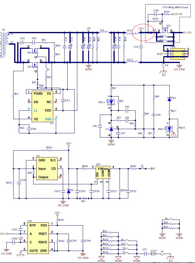
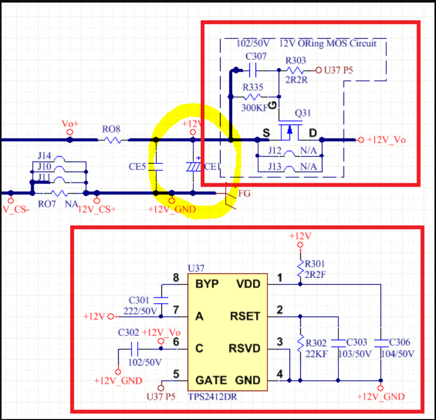
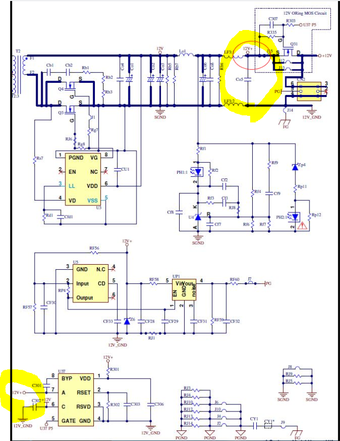
This thread has been locked.

If you have a related question, please click the "Ask a related question" button in the top right corner. The newly created question will be automatically linked to this question.

TPS2412: TPS2412 No gate single

Part Number: TPS2412

Hi TI Team,

I have a question about TPS2412 and please checks my customer application.

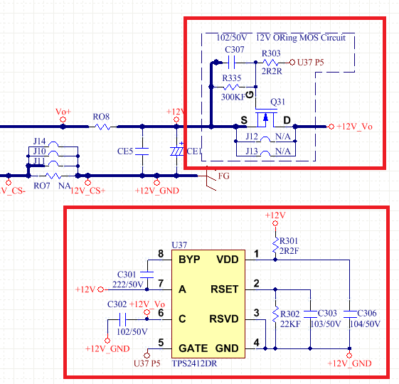
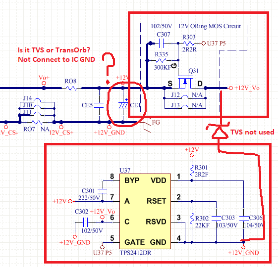
"Can be the TPS2412 Vdd powered form A as the red make?"

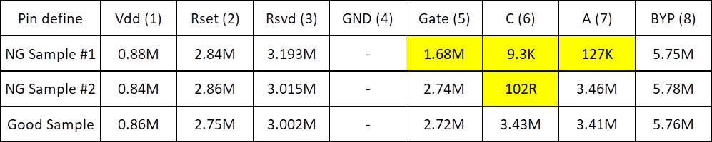
My customer found the IC broken of the gate PIN, there is no single after the function.
After A-B-A the PCBA can be work with a good IC.

The information as the blowing:
Topology: Flyback
Application: 12V
Check output overshoot voltage=13.2V
Check OVP voltage=14V

 If need more information please feel free let me know, thanks

Customer SCH

  • Hello Rock Shao,

    Vdd can be powered from "A" as marked in red by you.

    Yes we are looking into the schematic, but I don't see the component values for resistors, capacitors and MOSFETs used for the U37 ORing IC TPS2412.

    Does the failure happen in production test or during lab testing or any other scenario.

    If you can share the test condition before the damage, that will quicken the resolution of the issue.

    What is the exact scenario this fail happend?


    Regards,
    Kari.

  • Hi Kari,

    Thank you for your support, there are schematic and the A,C pin test waveforms in high/low AC line
    and the issue was happened in the production line ATE test after 4 hours burn-in and Hi-pot test .  

    If you need any waveforms to confirm this problem please feel free to let me know.

    TI-TPS2412DR Test Waveform 20200728.xlsx

    Thanks,
    Best regards

    Rock Shao

  • Hello Rock Shao,

    Thank you for sharing the details of the components used and the test results.

    Let me review this and get back tomorrow.

    Regards,

    Kari.

  • Hello Rock Shao,

    I have looked at the waveforms and see that A and C are shorted.

    Could you check if the MOSFET is damaged, also share the MOSFET part number as it is not seen from the schematic.

    Another possibility is over voltage at the input due to any transient spike at the input of the IC (18V is absolute maximum rating).

    I see that there are transorbs placed, but rating is not seen, can you share this as well.

    If any other pin of the IC is damaged, check and let us know.

    Regards,

    Kari.

  • Hi Kari,

    The MOSFET not broken, the customer has checked the NG PCBA can be work and normal with a good IC.

    And I don't know  "I see that there are transorbs placed, but rating is not seen, can you share this as well. " means. Could you mark in the schematic?

    The following is the impedance check between a good IC and NG ICs.

    Best regards

    Rock Shao

  • Hello Rock Shao,

    Thank you for sharing more test data on this one.

    C and A pins along with Gate pins are severely damaged and this can be due to over voltage (spike) exceeding the maximum ratings 18V of the IC.

    If over voltage spikes are seen when used with flyback converter output, recommended to have TVS at the A pin to Gnd and C pin to GND, to prevent transient voltages from damaging the IC.

    Please refer to the attached schematic picture with comments added (in Red Color).

    Regards,
    Kari.

  • Hi Kari,

    The red circle is the output capacitor, it's connected to the ground, you can check the following pictures, there are the same.

    Are the TVS need to have A pin to Gnd and C pin to GND both or choose one side? Which side is recommended? thanks.

    Thanks and best regards

    Rock

  • Hello Rock,

    Based on the failure data you have provided, both C and A pins along with Gate pins are damaged.

    But C pin is most severely damaged. Adding protection to C pin would help to prevent the failure if the failure is related to over voltage.

    Regards,
    Kari.