Other Parts Discussed in Thread: TPS51220
Hi Sir,
may we learn from you,
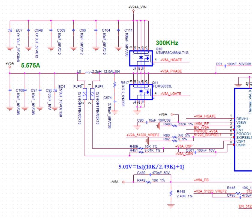
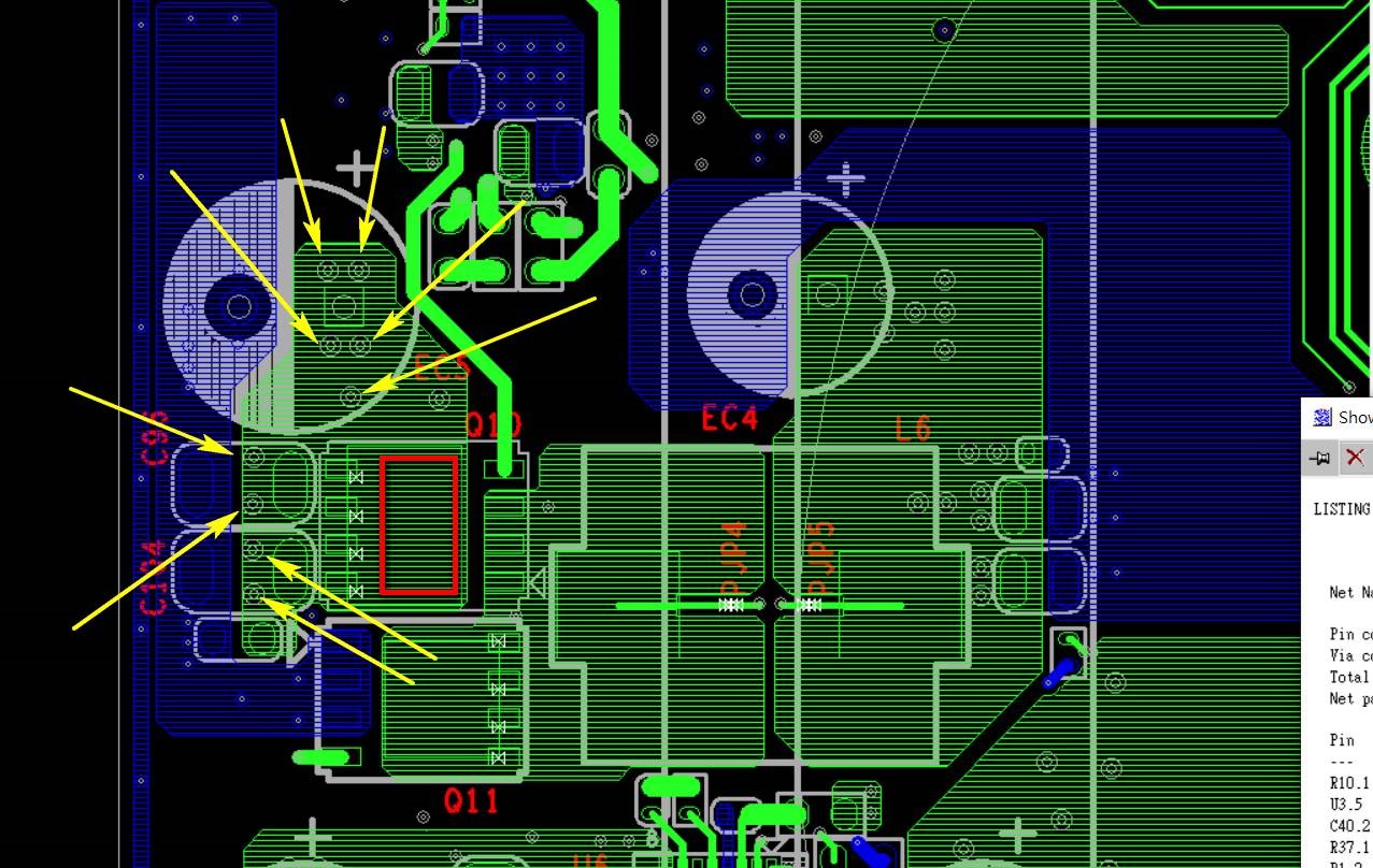
Please refer to below schematic and layout design.
there are some design concepts needed discuss
we design TPS51220 for +V5A at PHASE1
about the VIN ceramic bypass / High side Q10 / low side Q11 / output bypass ceramic and EC4
Question1
case I : the VIN was provided from internal layer through the via (yellow arrow)
case II: change those via holes from current location(yellow arrow) to high side Q10 Drain thermal pad
above design concept, which one can provide better power quality and reduce ESR/ESL
if there are any better location for those via holes, please suggest! thanks
Question2:
About the output by-pass solid Capacitor
Should we add some GND via for EC4 and output ceramic for power return path?
Question3:
PCB TOP side EC4, should we design pattern at TOP side under EC4?