This thread has been locked.

If you have a related question, please click the "Ask a related question" button in the top right corner. The newly created question will be automatically linked to this question.

WEBENCH® Tools/TPS61022: 3.7 v 0.5c 6000mAh Lipo battery input to 5 V 3 Ampere output design

Part Number: TPS61022
Other Parts Discussed in Thread: TPS61088,

Tool/software: WEBENCH® Design Tools

Hello,

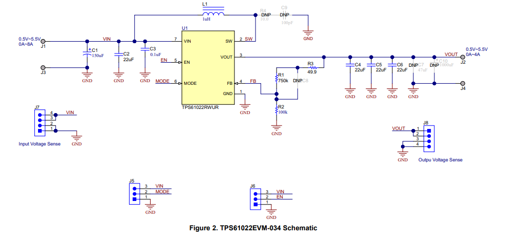
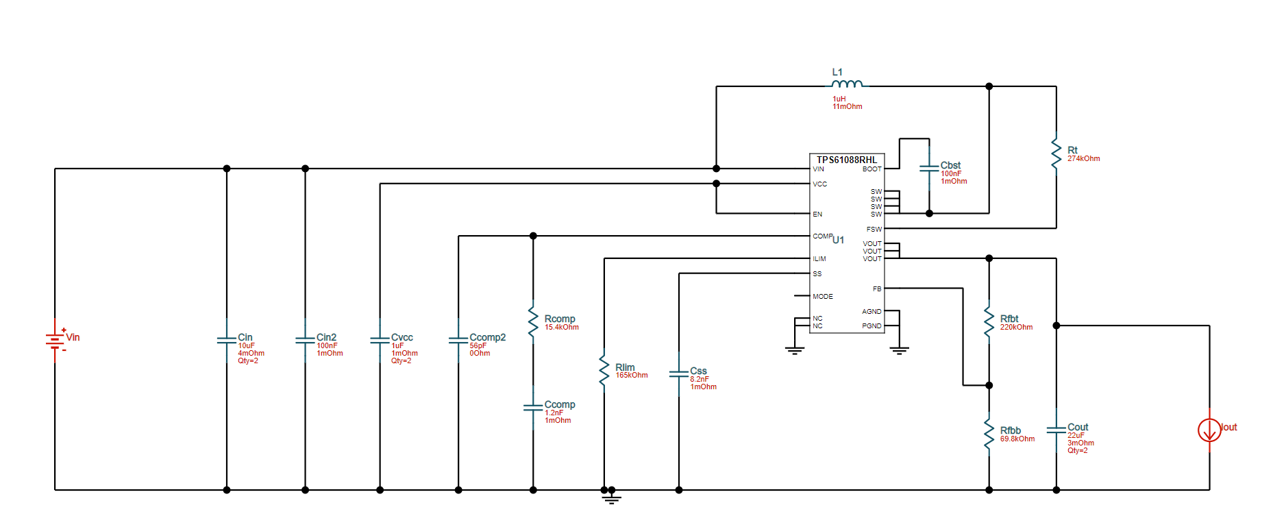
I was looking to design a boost converter so I looked up some sample designs from your TPS61022EVM-034 and webench design tool to find one appropriate from my application. I noticed some differences between the former and latter (attached below) and I would like some further explanation if that is possible. I was also looking at specifying whether the TPS61088 would be better suited for my solution as my load would be a smart phone device charger with 15 serial addressable WS2812B LEDs  and an Arduino nano v3.0 MCU unit.

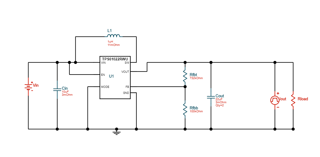
Comparing the evaluation module to the webench sample design for the TPS61022:

1) Why are the input capacitors in the evaluation module compared to the webench design so drastically different and would it affect the performance of my system if i follow the webench sample design for my specific application?

2)What should my FB voltage be to ensure a stable 5V 1.5A-3A output for my 3.7-4.2V 1.2A-3A single cell lipo battery. Also what is the purpose of R3 in the evaluation module's voltage divider?

3)Should mode be grounded for my application?

4) Is the extra 22uF output capacitor used to simply smooth the output signal or does it have to do with the frequency produced in cohesion with the 1uH inductor

5) Should i look at implementing a battery protection circuit to protect from undervoltage situations at the input of the converter since this is an ultra low voltage IC?

Thank you in advance for your feedback! 

  • Hi Ibrahim,

    1. The input capacitors are not critical for a boost converter. You can put two 10uF ceramic capacitors at input.

    2. R3 is used to measure bode plot. If you don't need to test bode plot, you can remove it. To output 5V, the correct feedback resistors are 732k and 100kohm.

    3. It depends on you. When MODE pin is connected to ground, the device works at auto PFM mode to increase efficiency at light load condition. When MODE pin connected to Vin, the device works at forced PWM mode at full load range.

    4. More output capacitors could decrease the output voltage ripple. If you hope a lower output voltage ripple, you can use three 22uF ceramic capacitors.

    5. You can disable the boost converter by setting EN pin to low when battery voltage decreases below 3.7V.

  • Hello Zack,

    I guess my next set of questions is:

    1) Would the chip considered to be more efficient if operating for a 3 A load at auto PFM or forced PWM mode?

    2) Is there a way to monitor battery voltage when its being discharged/charged continuously to setup the EN pin to be active low at voltages below 3.7?? Initially, I thought of some voltage divider circuit or MOSFET although I'm not sure if that would be the most accurate. Do you have any suggestions I could follow?

    3) Would the TPS61088 be a better suited IC for a 5 V 3A load output and 3.7-4.2 input and is the schematic above going to be sufficient to deliver my device's power needs efficiently?

    Thank you,

    Ibrahim

  • Hi Ibrahim,

    1. Yes. At light load condition, PFM mode efficiency is higher.

    2. Do you have a MCU on board to monitor the battery voltage? If not, there is another way. Please refer to the application note:

    3. TPS61088 maximum output voltage is higher with higher BVDSS MOSFET integrated. Both two parts have the ability for your application.