This thread has been locked.

If you have a related question, please click the "Ask a related question" button in the top right corner. The newly created question will be automatically linked to this question.

LM5025C: Broken Issue : Active Clump with UCC27200

Part Number: LM5025C
Other Parts Discussed in Thread: LM5025, UCC27200, LM5025B, LM5025A

Dear Expert,

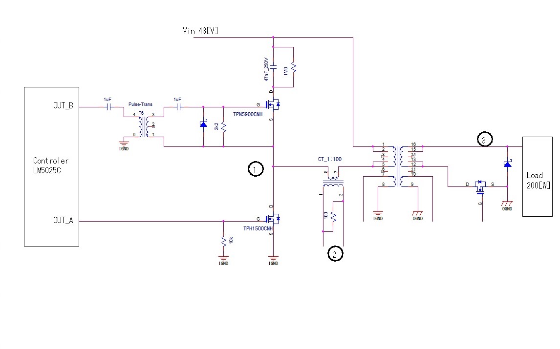
We are using LM5025 and UCC27200 together to Active Clump Converter and worry that UCC27200 has been broken when power down state.

We can not find reasons that PWM duty is increasing when power down, and occurred spike generation on HS of th gate driver over 120V even if we apply 48V Vin.

Attached schematics and Waveforms 1 is observation of broken and another is changed percentage of the load.

I appreciated if you give some suggestions to avoid increasing the duty and / or HS voltage when power down.

regards, Keiichi

200710.docx4786.200923.docx

  • Sorry I missed attachment file of the schematics.

    regards,

    ACF-PS_00-c_sch.pdf

  • Hi,

    Can you change C5 from 0.22uF to 0.1uF?

  • Thank you for your quick response.
    What kind of effects can we expect is we changed C5 capacitor value?

    Again I think you to know more clearly what's going on.
    Problem is during power down, gate driver reached broken when positive duty increase and voltage also increased, over 120V.

    Let me explain what waveform is;
    Upper picture is a case of broken UCC27200.
    We can see Voltage of SW-node exceeded 120V then Gate-driver has been broken-down, and maybe influences, Vdd become to higher for a while.

    Lower picture is a case of alive Gate-driver.
    It is kept less than 110V so gate-driver was NOT damaged.

    Our understanding of this broken issue, a cause of voltage increasing at Clamp side, when Vin is going to lower and duty is larger.

    Well in case large input voltage range (36V to 48V), can we avoid such as voltage increasing?

    200929.docx

  • Hi,

    First, please change C5 to 0.1uF so to make sure the damage not from 0.22uF as in general, UCC27200 boost strap cap value should not be > 0.1uF for its safety.

    Second, when you saw the 110V or 120V, were you power off your board, or what were you doing when you saw such high voltage? 

  • Dear Hong Hung

    Thank you for your reply.

    Per second article from you, we saw this phenomena when power down.

    When VCC is going down, PWM positive duty will be increased then voltage is also increased, in the results a gate driver reached broken....

    Vin range is 36V to 48V, and its spike voltage level is 110 to 120V.

    C5 should be changed to 0.1uF as you mentioned, are there alternative ways to avoid increasing voltage?

    regards, Keiichi Takahashi

  • Hi,

    If this is during power off and with Vin at what you described 36V to 48V, our experience is that the high voltage at the switch node is likely due to the secondary side energy regenerated back to primary side, but that is usually with self driven SR. But in your case, you are using LT8311 for SR driver. Then it looks you may need to adjust LT8311 setup so reduce the energy regeneration speed from secondary to primary.

    Can you ask support on LT8311 to tune up this device so to help to reduce the primary switch node voltage spikes during power off?

  • Dear Hong Huang,

    According to SR related, we tried to be disable LT8311 SR but behavior was same.

    Please refer to attached waveforms. You can see activated condition (upper) and disabled condition (lower).

    Therefore, there is no relation with secondary, we will not adjust SR.

    I would like to reconfirm this phenomena, do you agree to increase voltage of SW node when power down? 

    Reason is that PWM duty is increasing when power down, is this right?

    Go back to broken issue, we are now doing test many times(+0ver 500 times)  that UVLO is maximize against Vin.

    Then we can not see any behaviors to exceed absolute rating of the gate driver, it maybe solved issue.

    Do you think it is better solution ? Anyway boot strap cap will be changed next time.    

    Any other idea to reduce SW voltage when power down?

    201002.docx


  • Hi,

    Yes, increase UVLO off can help reduce the switch node voltage. This device maximum duty cycle increases when input voltage reduces, and this device maximum duty cycle can go as high as close to 90%. From the volt-seconds balance, Vds = Vin/(1-D), and your circuit shows UVLO pin with a capacitor, also introduce some delay, and high D (duty) is resulted and making Vds (or switch node voltage) high.

    LM5025A, and LM5025B has maximum duty 85%, and 71%, so < 90%, so if your design is ok with these duty cycle limits, you may consider to change to these. Also, reduce UVLO capacitance can also help.

    On the primary main MOSFET voltage you can ref the below article. 

    https://www.ti.com/lit/an/slua322/slua322.pdf?&ts=1589537651705


  • Dear Hong Huang

     We would like to draw some conclusions here. We hope that LM5025 and UCC27200 combination is appropriate and effective.

    We are trying to use TI's controller and gate driver, however have been plagued by problems between these two products.

    In the past, the symptoms on the primary side did not change depending on whether it was the SR or diode on the secondary side, so we decided to take measures only on the primary side.


    1. For Active Clamp, please answer that it is normal behavior that the phenomenon of duty increase and Vds voltage rise occurs when the power is shut down.

    2. In order not to exceed the absolute maximum rating of the gate-driver, please answer that it is protected by the method of maximizing UVLO in the current circuit.
    I think the circuit was already sent last Monday.

    Best regards, 

    Keiichi Takahashi

  • HI,

    1. For Active Clamp, please answer that it is normal behavior that the phenomenon of duty increase and Vds voltage rise occurs when the power is shut down.

    Yes, this depends the UVLO off instant and the device has no function to make its status right after UVLO off. 

    2. In order not to exceed the absolute maximum rating of the gate-driver, please answer that it is protected by the method of maximizing UVLO in the current circuit.

    Based on what you provided, It looks this is a maximum duty cycle design related matter. So increase turn-off voltage makes maximum duty cycle smaller then corresponding switch node voltage will become lower. 

  • I embedded paragraphs into your comments below.  Refer to schematic that I have sent as attached file last month. 

    HI,
    1. For Active Clamp, please answer that it is normal behavior that the phenomenon of duty increase and Vds voltage rise occurs when the power is shut down.

    Yes, this depends the UVLO off instant and the device has no function to make its status right after UVLO off.

    >>> I need your comment generally, for Active clamp. "Yes" means am I right?

    2. In order not to exceed the absolute maximum rating of the gate-driver, please answer that it is protected by the method of maximizing UVLO in the current circuit.

    Based on what you provided, It looks this is a maximum duty cycle design related matter. So increase turn-off voltage makes maximum duty cycle smaller then corresponding switch node voltage will become lower.

    >>> Would you please tell me more, which voltage did you mentioned "turn-off" voltage ? Is this UVLO?

          Still any other problem or there is no problems? 

    We have to close these issues as soon as we can. First broken issues has been solved and we would like to lock current schematic.
    We have to mention that its schematic is safe using TI's products combinations. Your cooperation is very helpful.
    regards, Keiichi

    e2e.ti.com/.../ACF_2D00_PS_5F00_00_2D00_c_5F00_sch.pdf

  • My questions are embedded at post at Oct 7, 2020 10:21 AM, would you please comment again? We have to clarify  and we need to indicate "safety product" .

    regards, Keiichi 

  • Hi,
    1. For Active Clamp, please answer that it is normal behavior that the phenomenon of duty increase and Vds voltage rise occurs when the power is shut down.

    Yes, this depends on the VCC UVLO off or line UVLO off instant and the device has no function to make its status right after UVLO off. This is normal on this device, and should not cause any issues in a design.

    2. In order not to exceed the absolute maximum rating of the gate-driver, please answer that it is protected by the method of maximizing UVLO in the current circuit.

    Based on what you provided, It looks this is a maximum duty cycle design related matter. So increase turn-off voltage makes maximum duty cycle smaller then corresponding switch node voltage will become lower. You need to design the maximum duty cycle to resolve this or you can also make design along with the transformer turns ratios so to the maximum duty cycle can be lower so not to make the clamp voltage so high to exceed the limit for other devices such as UCC27200.

    >>> Would you please tell me more, which voltage did you mentioned "turn-off" voltage ? Is this UVLO? You can take look at the application note from this link on maximum duty cycle and the clamping voltage for this.https://www.ti.com/lit/an/slua322/slua322.pdf?&ts=1589537651705

          Still any other problem or there is no problems? I do not see other issues based on your tests and feedback. In the meantime, the UCC27200 bootstrap capacitor value should be changed to 0.1uF.

    We have to close these issues as soon as we can. First broken issues has been solved and we would like to lock current schematic.
    We have to mention that its schematic is safe using TI's products combinations. Your cooperation is very helpful.