Hi TI,
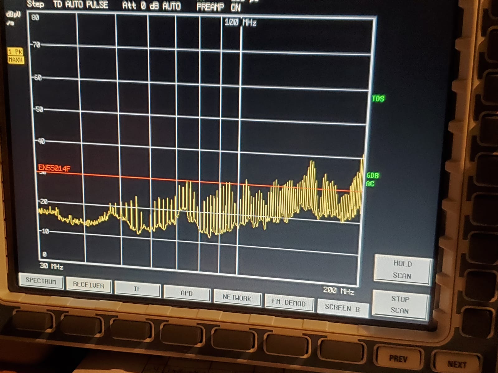
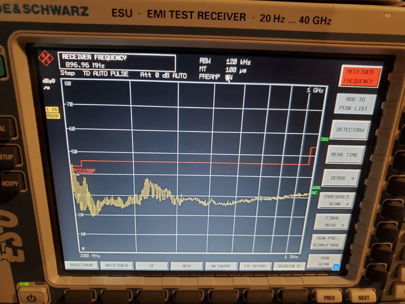
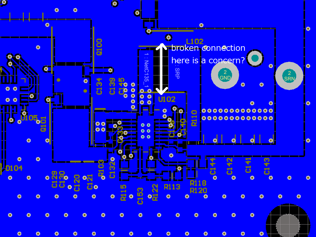
We are having radiated emission issue in both FCC and CE testing with using this charging IC.
We have tried adding common mode chokes for improvement but without much success.
Can help to review the schematics and layout and provide any suggestions for improvement??
The configure are as follow:
15V USB PD input, 1.8A charging for a 3S2P 18650 lithium battery pack.
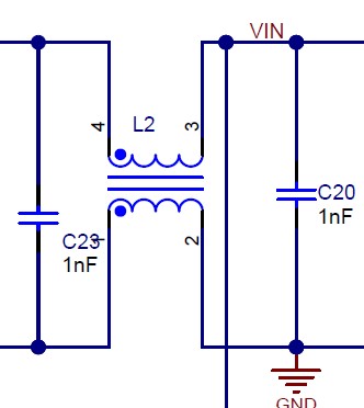
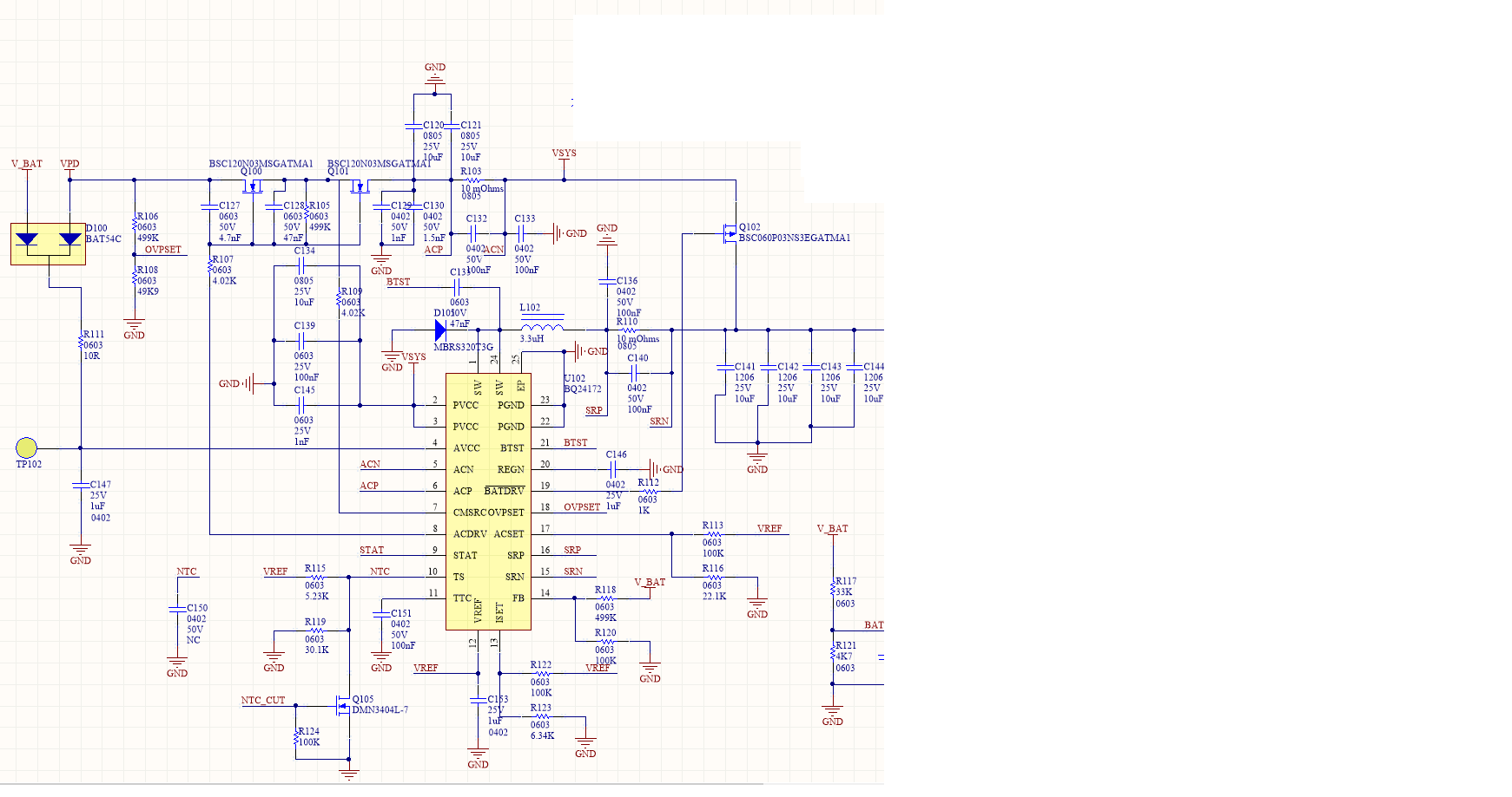
Charging schematics:
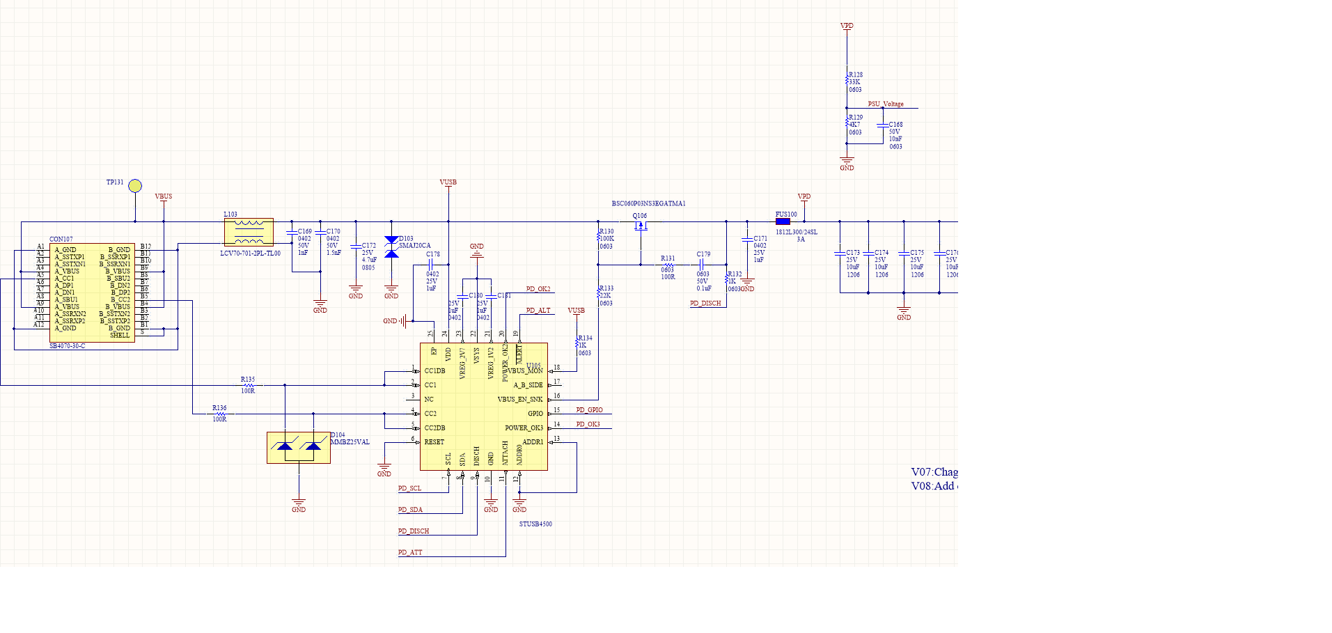
PD input
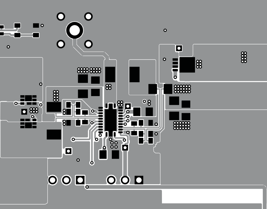
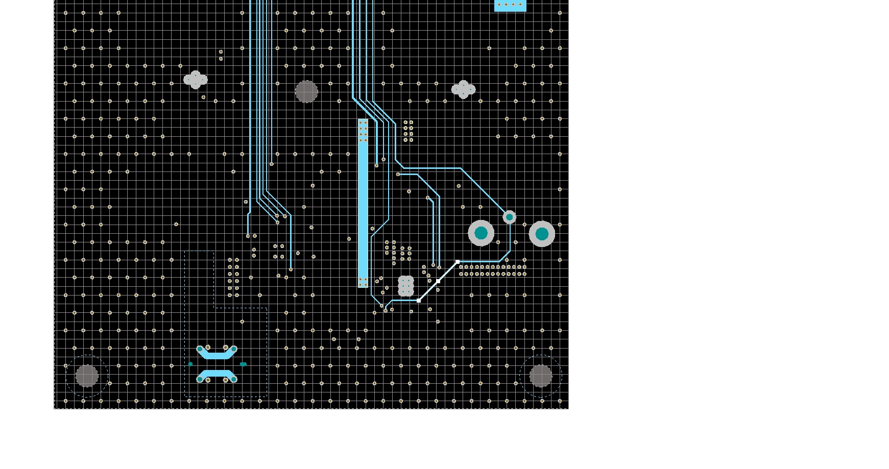
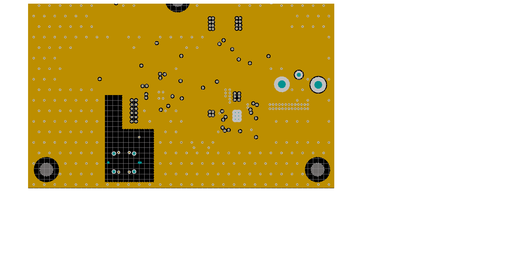
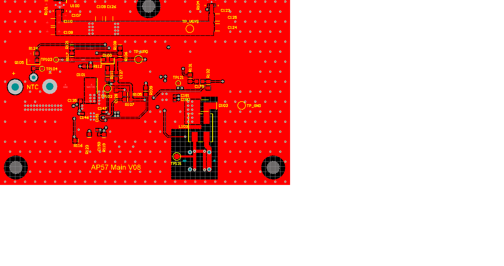
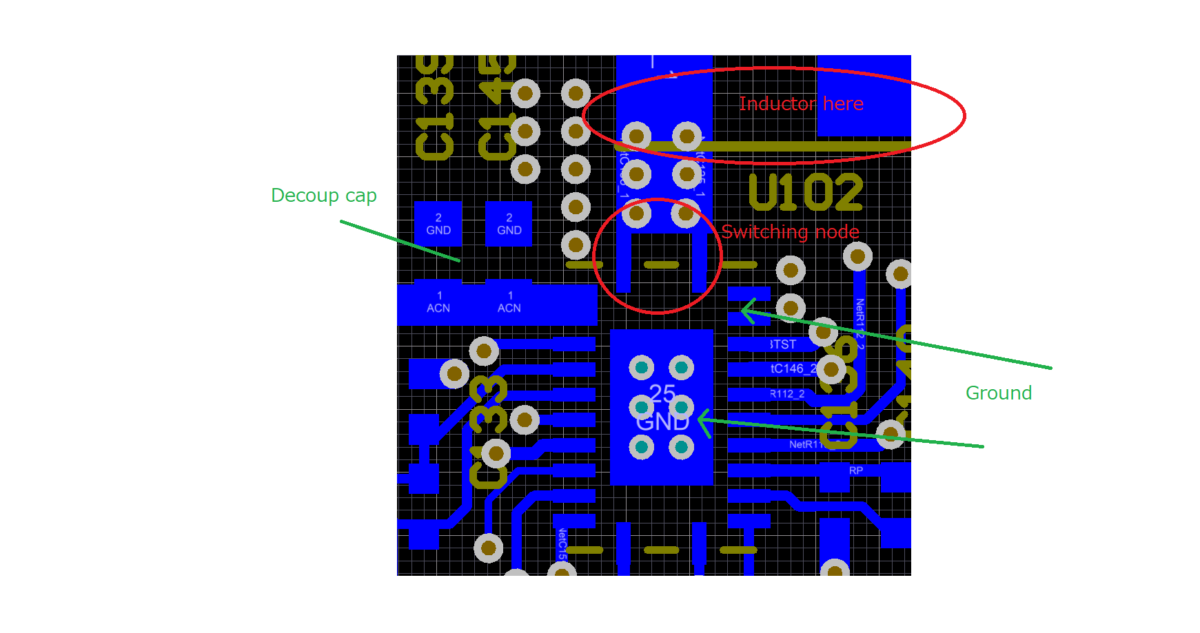
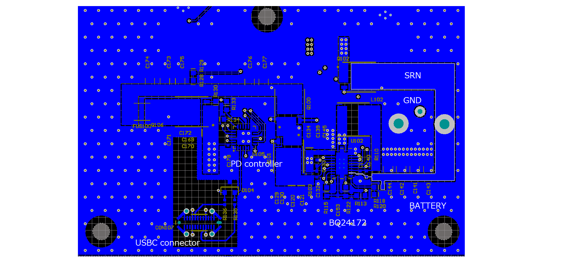
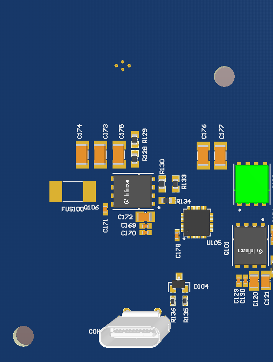
Layout
PCB 3D
EMC results: