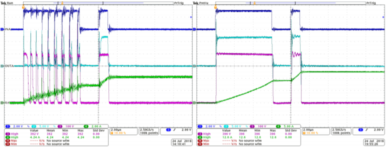
All inputs need to be properly filtered to create a robust system. Improper input filtering can lead to a variety of undesirable effects as a result of electromagnetic interference (EMI) from power stage transient voltages and currents. Figure 1 shows a double pulse test where there is no input filtering on the left and proper input filtering on the right. Further details on input filtering can be referenced in the linked application note (link).
Figure 1: Effects of input component filtering on input pins (no filtering on left, proper filtering on right)
- Disable (DIS) Pin and INx Pins:
Noise from the driver pin can couple onto the input pins (DIS/INx), causing the driver to react to transients instead of PWM signals. This can result in unwanted behavior on the driver input and output, as well as reduced system performance. In addition, increasing the distance between the DIS pin and the driver requires more caution for layout and filtering in order to avoid this unwanted behavior. If the disable function is required, use a low ESR/ESL capacitor with a value of approximately 1nF for overall improved system performance as seen in Figure 2.
For filtering the INx pins, use an input resistance, RIN up to 100 ohms and an input capacitance, CIN ranging between 10 pF and 100 pF (see Figure 2). Keep in mind that when selecting filtering components, it is important to pay attention to the trade-off between signal integrity and speed (propagation delay), as a delay is introduced from the RC filter time constant.
Figure 2: Example of proper filtering for DIS/INx pins
- No Disable required:
If no disable is required, tie the disable pin to GND in order to deactivate this function and to achieve better noise immunity as shown in the figure below.
Figure 3: Deactivation of DIS pin by tying to GND
- Floating deadtime pin
A floating DT pin should be avoided to prevent noise from coupling in and disturbing the dead time duration.
Figure 4: Floating deadtime pin
- Programmable deadtime
If programming the deadtime through a deadtime resistor, place a capacitor in parallel with a value greater than 2.2nF to increase noise immunity during fast switching transients as seen in the figure in the middle.
Figure 5: Example of proper filtering for DT pins
- No deadtime
If no dead time is required, tie the dead time pin to VCCI to deactivate the DT circuit.
Figure 6: Deactivation of DT pin by tying to VCCI pin
Achieving best system performance with high power gate drivers requires attention to detail. In order to maximize performance and efficiency, there are several design considerations and best practices to keep in mind, and by implementing proper input filtering, designers can ensure the best overall system performance.


