This thread has been locked.

If you have a related question, please click the "Ask a related question" button in the top right corner. The newly created question will be automatically linked to this question.

TPS65279: Troubleshooting Constant Current Feeback issue

Part Number: TPS65279
Other Parts Discussed in Thread: INA139, TLV4333

Hello,

I'm looking for some assistance troubleshooting a TPS65279 circuit that seems to keep going into OVP or OCP whenever it is attached to a load.

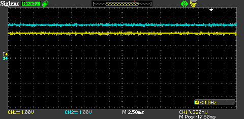
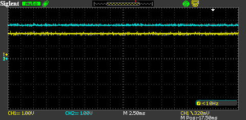
When no load is attached it operates as expected (swings to VIN at the output). When the load is attached (in this case a diode load Vf = 2.5V) the output never seems to rise above 1.5V, and no current flows.

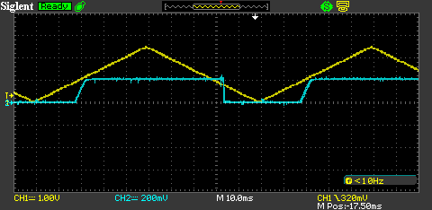
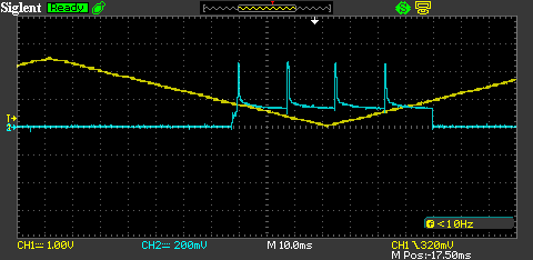
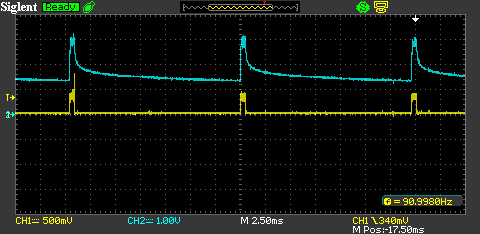
I decided to scope SS pin (yellow) and VOUT (blue) and you can see the behavior here:

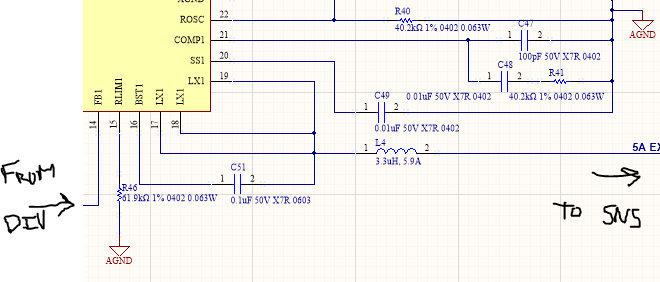
Since the OSC is 1MHz, (1us cycle) What I believe im seeing is the 512 us cycle hiccup wait time followed by the 16384 us shutdown/restart hiccup time. That would be an overall period of 16896 us (16.896 ms)  or the roughly  ~17ms im seeing here. I've been reviewing Section 8.3.7.2 Low-Side MOSFET Overcurrent Protection in the TPS65279 datasheet and it specifically mentions that the output overload condition is measured by the COMP pin. 

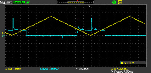
My COMP pin never seems to rise above 75mV, also indicating a overload condition.  I took note that my RLIM is set to 7.26A (61.9kOhm) for this channel, and I see that datasheet notes the I_LIMITLSx low-side sink current to be -2.6A, but I do not see what the low-side *source* current limit is.

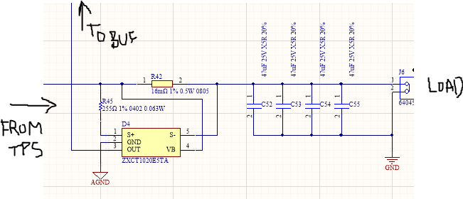
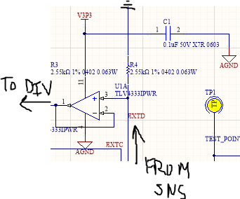
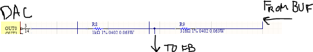
The sensing feedback circuitry uses a high side current monitor (similar to the INA139), a unity gain op amp buffer, voltage divider (for V_fb) and a voltage DAC. Since there is negligible output current from the TPS65279, the output of the divider never reaches the 0.6V reference voltage.   

Any direction would be appreciated.

  • Hi, sir 

    1. Could you send me your schematic? 

    2. What is your application? why do you design a high side current monitor? what does it used for? 

  •  

    1. It may be easier to convey the just essentials here for a single channel, since I believe this is related to the COMP network.


    The output of inductor L4 in this image is connected to the high side of the ZXCT current sense. (Functionally it is similar to the INA139 device, but its what I had leftover from another design). The 255 ohm and 2.55k produce a resultant gain of 10. The current sense voltage OUT is buffered through the TLV4333 device. The load is connected to J6 in this image.

    Finally, the resistor divider network is setup 1k : 316 ohm. This is because the reference of the DAC is 2.44V

    So when DAC = 2.44V, OUT =  0.01856V, FB = 0.6V and when DAC = 0V, OUT = 0.7896V, FB = 0.6V

    This gives OUT = 10 * Iload * Rsense . (Again, gain is 10 here, and Rsense = 0.016 ohm).

    So OUT/(0.16) = Iload.

    The expectation would be then that when DAC = 0, Iload = 4.935A, and when DAC = 2.44, Iload =  0.116A

    2. This particular application is a generic constant current source with analog modulation.

  • Hi, Sir 

    Thanks for explanation, it is very clear. 

    I think the problem is probably at compensation circuit. 

    I suggest changing R41=2.7kohm that is same with EVM's value. 

  •  

    Thanks for the quick reply. 

    That was my thinking initial as well. I tried an experiment where I replaced the R41= 40.2k with one of my 2.55k resistors, since that was close and on hand - and saw no significant difference. I'm happy to try again and pass along some scope traces.

    Moreover, I selected my COMP values based on the instructions given in the datasheet.

    Where nominally I expected my Vf range for my loads to generally fall between 1.8V and 5.5V when operating at full current (5A).

    Using the equation for R_c given in 9.2.1.2.7 Loop Compensation of the datasheet, where

    R_c = ( 2*pi*f_c*V_o*C_o ) / (g_m * V_ref * g_mps )

    where

    g_m = 1350 uA/V

    V_ref = 0.6 V

    g_mps = 10 A/V

    C_o = 4 * 47uF = 188uF

    I back calculated using 50kHz < f_c < 200 kHz since thats 1/20 and 1/5 as the min/max crossover frequencies recommended. Based on my OSC of 1MHz

    R_c1 = ( 2*pi*50kHz*5.5V*C_o ) / (g_m * V_ref * g_mps ) = 39838.1997 ohms = 39.8k

    R_c2 = ( 2*pi*200kHz*1.8*C_o ) / (g_m * V_ref * g_mps ) =  52151.8251 ohms = 52.2k

    So I selected 40.2k since it was convenient (used for ROSC) and was R_c1 < 40.2k < R_c2

    Likewise, most of my Loads are diodes or TEC devices, with R_L on the order of 1 ohms. So I selected R_c based on that. 

    where the datasheet specifies:

    C_c = R_L * C_o / R _c 

    selecting 2 ohms for R_L yeilds:

    C_c = (2ohm* 188 uF) / 40.2kohm = 9.35323383 nF. So I selected C_c = 10nF

    while optional, chose C_b the same way.

    4 ceramic X5R capacitors in parallel have a low resultant R_ESR. Assuming 0.100 ohm ESR each, results in R_ESR = 0.025 ohm

    C_b = R_ESR * C_o / R_c

    C_b = (0.025ohm* 188 uF) / 40.2kohm = 116.915423 pF. So I selected C_b = 100pF

  • Hi, Sir 

    1. The calculation is correct. 

    Rc value determines the bandwidth of loop, but when bandwidth is large, it is very sensitive to noise when layout is bad, so i suggest reducing its value. 

    2. After changing, suggest probe some waveforms: 

    LX1, Comp1, Vout1. 

    3. For debugging, suggest making the TPS65279 stable first. 

    Set DAC=0V, and bypass SNS and BUF circuit, check if TPS65279 is stable or not. 

    After that, add SNS and BUF circuit back, and check again. 

  •  

    Just a quick update.

    Over the weekend I performed a basic test by bypassing the BUF and SNS circuit as you suggested, and I opted not to reduce the value of Rc at first for this test. (Rc = 40.2k)

    I used 40.2k for R1 and 12k for R2.

    Where Vout = (R1/R2)(0.6) + 0.6 = (40.2/12)(0.6) + 0.6

    Vout = 2.61 V

    Again, I probed SS (yellow) and VOUT (blue). First with no load.

    Next again with a Load.

    The TPS65279 is stable and produces the expected output (measured 2.626V at VOUT, measured 1.915V at SS).

    I was thinking the next test I may try is increasing the resistance of the DIV circuit. Currently it is 1k: 316, but I will try increasing it to 10k : 3.16k or 100k : 31.6k which maintains the same ratio with larger resistances. Thoughts?

  •  ,

    Thinking more about the DIV circuit, I think raising the impedance will address the problem. The output impedance of the DAC is very low (0.1 ohms) but the output impedance of the TLV4333 is comparatively very high (2k ohms).

    So with the TLV4333 driving the 316 ohm side of the 1k:316 divider, I believe that is where the problem is.

    I suspect I need values to be 10  to 100 times (20k to 200k) that of the output impedance of the TLV4333 so 100k and 31.6k are likely the better choice here, potentially even higher than that.

    I'll set up the experiment to test that out if you agree.

  • Hi, BGX 

    I totally agree with you. 

    In other words, the TLV4333 has limitation on output current and output voltage swing. 

    As you said, agree on increasing divider resistor to 100k: 31.6k, or 50k: 15.8k. 

  •  

    Following up on this. I performed the experiment with the DIV change, and re-add of BUF and SNS circuit. Once with 316k : 1M (1000x) and again with 31.6k : 100k (100x). Both of them performed better (as in the did not immediately shut down), and similarly -- however I am still continuing to see issues.

    I setup a function generator to output a triangle wave (as my DAC input) with a 2.44V max and a 0V min at 10Hz.

    DAC input (yellow) with respect to SS (blue). Notice there is a period when SS is low, and another when SS is high. This is the same hiccup overcurrent issue as before when SS is low, but there is a small range where current output is controlled. I would have expected SS to be about 0.6V, but as you can see here it is roughly 200mV.

    DAC input (yellow) with respect to VOUT (blue). Notice that again we have the same 17ms (approximate) hiccup time overload behavior at VOUT whenever the DAC input falls below roughly 800mV and the output completely turns off whenever the DAC exceeds roughly 800mV.


    Reducing the frequency to 5 Hz causes more instances of the overload condition.

    Reviewing these, it seems like The divided down DAC is somehow being used as my VFB. Since SS is approximately 200mV, it makes be believe that's somehow my internal reference. If it is, it would make sense that it would "turn on" below roughly 800mV because (0.200)*(100k+31.6k)/(31.6k) = 0.833 V 

    Since 0.2 is far below 0.6 it enters overload. Possibly?

    Still trying to figure out why this isn't being controlled as expected. 

  • Hi, BGX 

    It seems the FB voltage cannot follow the SS voltage during soft start, the big (SS-FB) voltage will lead to big comp voltage, then trigger OCP.   

    Could you send me whole schematic? I want to double check it, and want to do some simulation. 

  • I can send it your way, just let me know where to send it.

    Thanks

  • Hi, BGX 

    You can attach it here or send me the email: zhao-ma@ti.com. 

  • Hi, BGX 

    Let's talk about this issue by email.