This thread has been locked.

If you have a related question, please click the "Ask a related question" button in the top right corner. The newly created question will be automatically linked to this question.

TPS61391EVM-058: Effect of loading

Part Number: TPS61391EVM-058
Other Parts Discussed in Thread: TPS61391, OP07, TINA-TI, TPS61390, TPS65132, TPS65133, TLV751

Hello there,

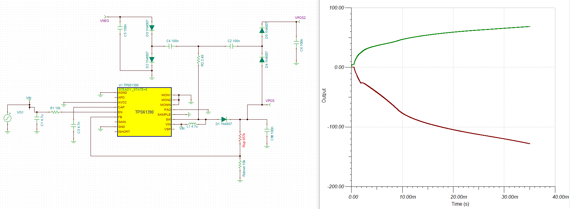
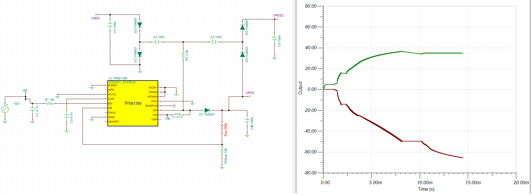
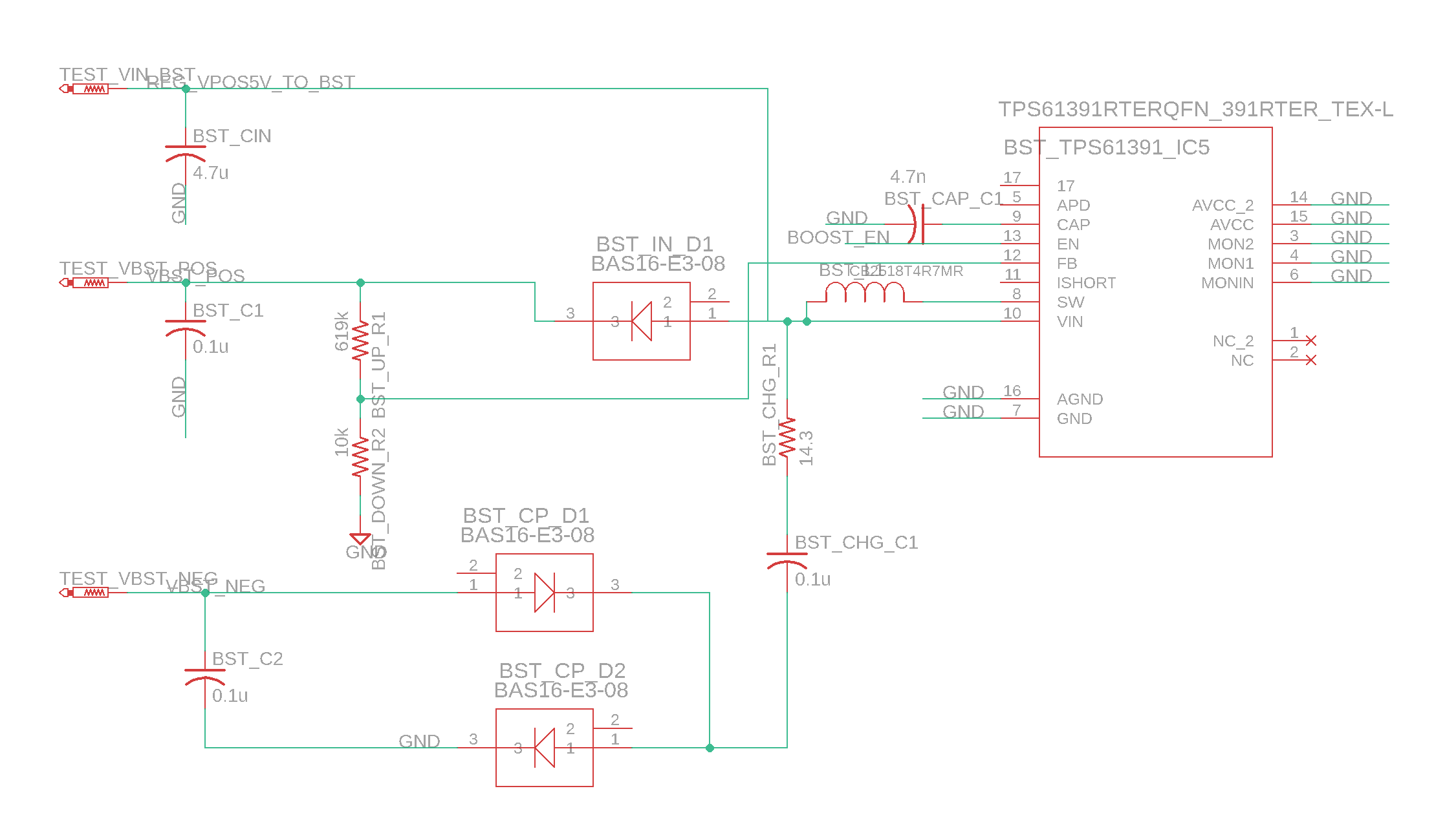
I am evaluating the TPS61391 boost converter with the corresponding evaluation module. I am using the boost converter to supply high voltage compliance power rails to an op-amp based V-to-I converter. WIth the resources I have on hand, here is what I did:

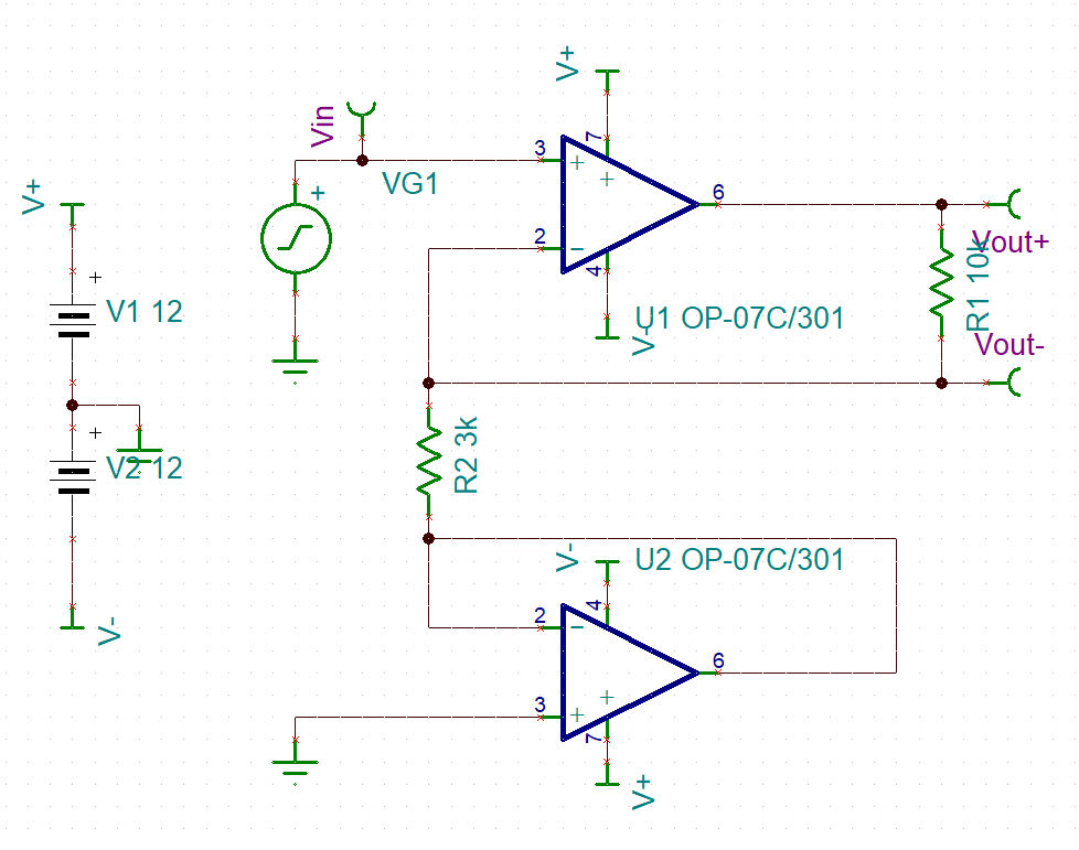
1. I am using the OP07 op-amp.

2. The boost converter EVM is powered by 5V supplied through a USB+ voltage regulator.

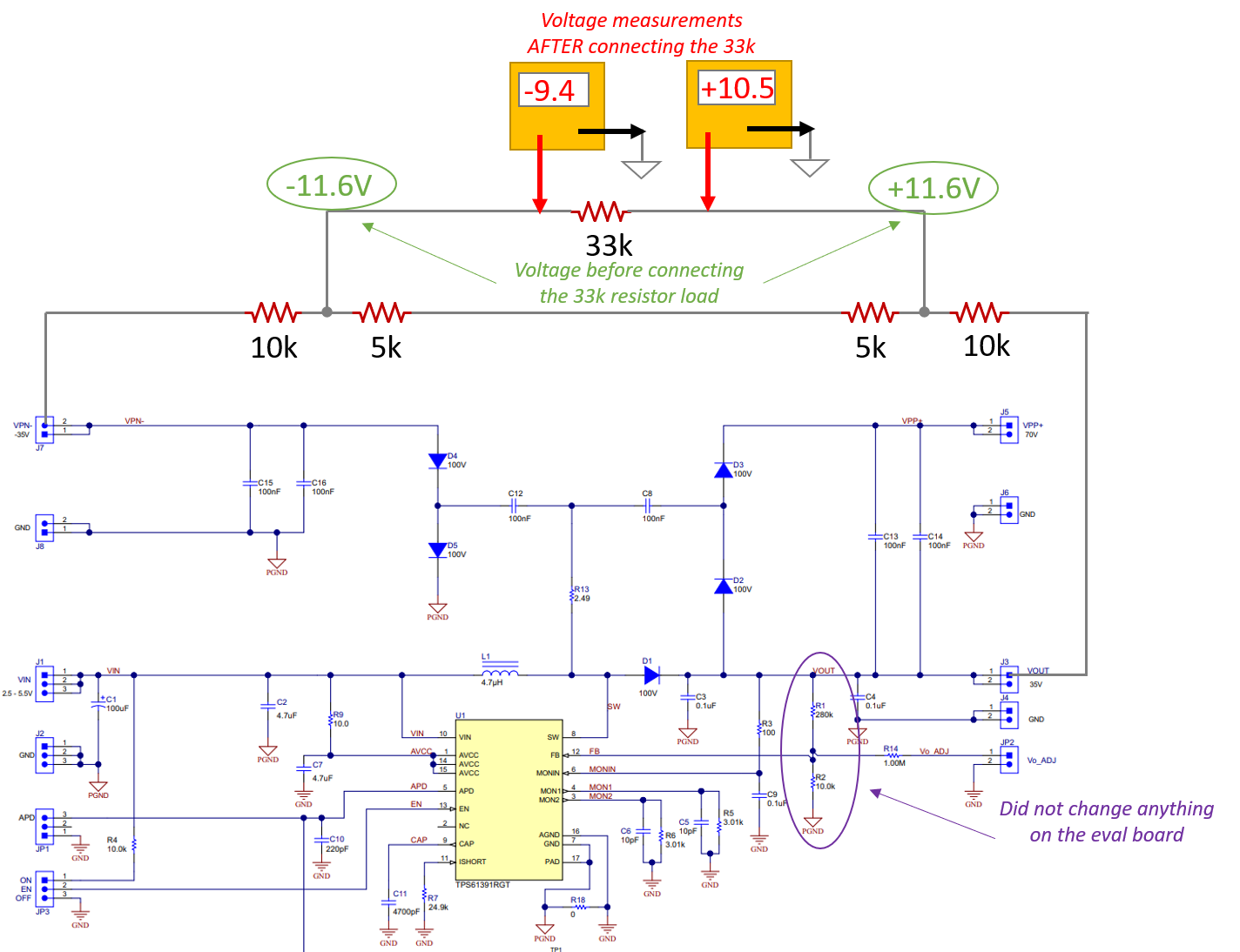
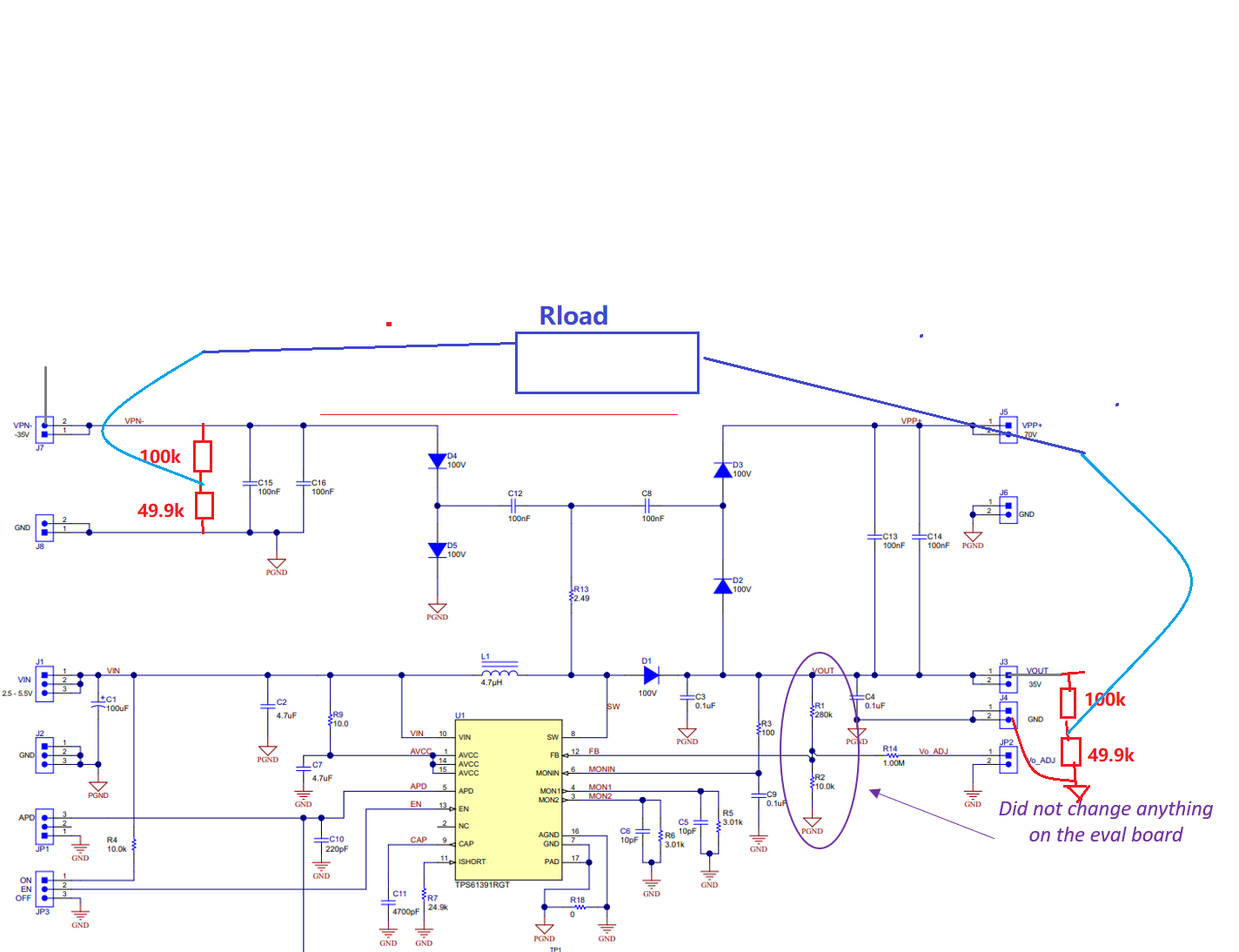
3. On the EVM, I have stepped down about a third of the voltage as supply to the OP01. The +35V (from VOUT) to +11.6V and the -35V (from VPN-) to -11.6

4. I connect the V+ and V- of the op-amp accordingly to +11.6V and -11.6V.

Here is my issue:

As soon as I connect the power rails from the stepped-down boost converter to the op-amp and measure the power supply pins of the op-amp - it reads a much lower voltage than +/- 11.6V, for my V-to-I circuit, it measures +/-4V.

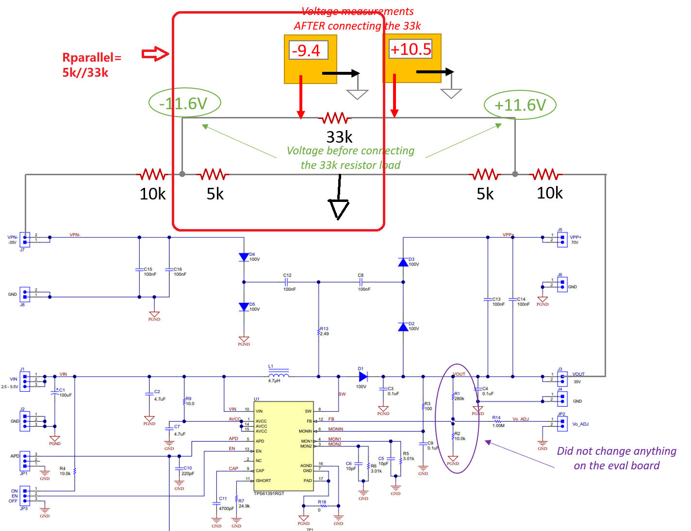
To double check, I connected a 33k resistor across the +11.6V and -11.6V, the voltage at those pins now read +10.6 and -9.3V instead. 

I would like to understand what is happening here, an op-amp shouldn't be loading down a boost converter designed to supply 1000mA, let me know if I should be doing something differently.

Thanks!

Ashwati

  • Dear Sir,

    It can load +11.6V and -11.6V  /25mA load current.

    What is the consumption current of OP07 op-amp?

  • Hello Helen,

    The OP07 does not have a specific current consumption spec - the bias current and offset current are in the nA range. I also tried the 741, and the voltage drop goes from +/-11.6V to ~+/- 5V.

    Here is another scenario:

    1. The Boost converter EVM supplies +/- 35V.

    2. I use a 5k/10k resistor divider to drop the voltage down to +/- 11.6V => current draw for divider circuit is 2mA (35/15k) x 2 = 4mA (max)

    3. I put a 33kOhm resistor across the power terminals, which means the circuit is supposed to draw 0.7mA (23.2/33k), the voltage across the resistor is now +9.7V and -9.5V.

    The loading is happening even for a resistor.

    Big picture: Here is what I am trying to do with the TPS61391:

    1. I am trying to use the TPS61391 as the power rails of a V-to-I converter circuit, to increase the voltage compliance of the current source. 

    2. I am pasting an image of the V-to-I circuit here:

    My questions:

    Q1. Why is the TPS61391 loading even for a resistor, when I am not drawing current even close to the specified limit of 1000mA - have I misunderstood something?

    Q2. Based on my big picture description, if the TPS61391 is not the right chip, what other chip can I use to increase my voltage compliance to about 70V?

    Thank you,

    Ashwati

  • Dear Sir,

    How did you change the board? please refer to the attached schematic. you just need to change the upper side dividing resistor to 86.6k .

    Thanks!BMC058A(001)_Sch.PDF

  • Hello Helen,

    I apologize if my description was not clear enough. I did not change anything on the Eval board, here is a rough schematic of my connections and the issue that I am trying to describe. Just make sure we're on the same page, and explain to me how changing the resistor on the Eval board will prevent the loading that I am seeing. I understand that changing the resistor as you suggested will reduce the output voltage value, however, that is not the issue I am trying to highlight. Let me know if this schematic makes it clearer:

  • Dear Sir,

    In your connection, the equivalent resistance is smaller than 5k, so you can't get -11.6V voltage.  Please change the feedback resistance of R1 and R2.

  • Hello Helen,

    Just to clarify, I made a mistake in my first figure that you have corrected. As you have drawn, I did connect the voltage dividers to ground respectively, but I forgot to draw the ground, it is where you have drawn it.

    Can you please elaborate on the reasoning between the 5k equivalent resistance and the resulting supply voltage?

    If I understand correctly, you are asking me to change the feedback resistor to directly supply +/- 11.6V rather than use a voltage divider? Yes, this would be ideal, but currently under lockdown, my resources are not the same, therefore I was trying to step down the +/- 35V to something my op-amp can tolerate :).

    Thanks!

    Ashwati

  • Hi Ashwati,

    But your circuit is much more complex than just change the R1/R2.

    Based on the EVM, you just need to change R1 to 90.9k, which is pretty easy. 

  • Hello Helen,

    I feel like I have not communicated my main issue properly:

    1. I know I can change the resistor on the board, in my final design that is what we will do. However, I don't care about the value 11.6V, it was a stop-gap way to bring the voltage down to something the op-amp will accept. However, there was loading, which is why I started this thread. I do not have the tools to change an SMD part right now due to the lockdown.

    2. Can you please explain to me WHY the boost converter gets loaded even though I am not drawing the rated current of 1000mA? It shouldn't happen for the op-amp or the resistor. What is the 1000mA current rated for? Is it the current mirror or the boost circuit? What is the current draw limit for the boost circuit?

    Thanks,
    Ashwati

  • Hi Ashwati,

    Please check my reply below:

    1. I know I can change the resistor on the board, in my final design that is what we will do. However, I don't care about the value 11.6V, it was a stop-gap way to bring the voltage down to something the op-amp will accept. However, there was loading, which is why I started this thread. I do not have the tools to change an SMD part right now due to the lockdown. -> Understand. 

    2. Can you please explain to me WHY the boost converter gets loaded even though I am not drawing the rated current of 1000mA? It shouldn't happen for the op-amp or the resistor. What is the 1000mA current rated for? Is it the current mirror or the boost circuit? What is the current draw limit for the boost circuit?  -->1000mA means the peak inductor current , it is not the load current.  Since the converter works in the DCM mode, the inductor current is pretty  high even with a small load current.   In your application, the maximum load current can be around 30mA for +- 11.6V rail, and under this maximum load current, the peak inductor current is around 1000mA. 

  • Ah! Thank you for that explanation, Helen, it makes things a bit clearer. I still have a couple of questions:

    1. Based on your description, at +/-11.6V, the chip can support 30mA. However, with the voltage divider, there was a total current of 4mA (described earlier), and adding just a resistor load (33k) drew 0.7mA, which is a total 4.7mA, which is still less than 30mA. So this is still puzzling me.

    2. Is there a prescribed way of loading this circuit that you would recommend?

    3. Is there a graph of how much current the TPS61391 boost converter can support at different voltages? In our design, we would like to have upto 80V VOUT with a peak of 2mA, can this be supported?

    Thanks Helen,

    Ashwati

  • Dear Sir,

    Please try below circuit to see whether this could be helpful.

    TPS61391 can support 80V/2mA. But if it is +-80V/2mA, it should be OK, but no big margin .

  • Hello Helen,

    Thank you for getting back to me with the suggestion. I tried your circuit, it loads down the 11.6V to about 3.6V, but I imagine (similar to what you suggested earlier) that it is because the load resistor changes the effective resistance of the voltage divider (when looking from the output). Moreover, I also found an issue with the power supply that I was using, so I am not able to power an IC without an issue. Thank you for keeping track and responding.

    I had another question about the TPS16391:

    Can I set the output to be 70V on the chip by setting the resistors R1 and R2 (similar to 35V on the eval board), and then:

    (a) generate +140V using the voltage doubler (D2,D3) diode circuit,

    (b) -140V (like D4, D5 but 2 times instead of just an inverse) using a voltage quadrupler?

    My target is to be able to deliver 2mA at +/- 140V.

    Is there any limitation to doing this? Do you have any suggestions?

    Thanks!

    Ashwati

  • Hi Ashwati,

    sorry for the late as Helen just left TI.

    for  the 2mA +/- 140mV application, I'm concerning about the current capability of the device and the circuit would be complex.

    I would suggest you simulate the circuit with PSPICE firstly to evaluate the feasibility and then try with EVM.

  • Hello Jasper,

    Thank you for getting back to me - I had asked this question earlier as well - is there a model/macro I can use with TINA-TI for the 61391? I have looked through the SMPS macros I don't see it. Could you send me a macro to use if possible?

    Thanks!

    Ashwati

  • Hi Ashwati,

    please use the pspice model of the TPS61390. the behavior is the same.

  • Hello Jasper,

    Thank you, I was able to import the TPS61390 Pspice file into TINA-TI. I can now verify the functionality of my circuit as well. 

    Ashwati

  • Hello Jasper,

    I had one more question - do I need to connect the components for the APD current mirror if I am not planning to use that part of the circuit? I only need the boost converter to hit up to 80V.

    Thanks,
    Ashwati

  • Hi Ashwati,

    please refer to the application note https://www.ti.com/lit/an/slvaez7/slvaez7.pdf for the connection for pure boost application.

  • Hello Jasper,

    Oh this is very helpful - it also answers another question I had about exceeding voltage levels using the charge pumps. Thank you very much.

    Ashwati

  • Hello Jasper,

    You have been very helpful, I have a couple of questions more. I looked at the schematic in the application note you sent. There are a couple of issues I am having with the simulations:

    1. I am trying to generate a +/-80V output (Rup=657k; Rdown=10k) rail to support at least 5mA to the load.

    2. The circuit does not saturate, it keeps going - what should I be looking at to debug? (see the snapshot of circuit + output below)

    3. To compare, I also simulated Vout=35V ((Rup=280k; Rdown=10k; similar to the EVM, because I know that hardware is able to produce +/-35V), and the simulation snapshot is below - the positive voltage is stable, but the negative voltage keeps going - not sure what I have missed):

    4. The transient simulation is quite slow - is this normal? I assume so because the frequency of operation is 700kHz. Is there anyway to speed it up? Also, the time for saturation doesn't seem to match the oscilloscope outputs in the application note (it reaches -90V in 5-10ms). Again, is there something I am missing, or can do to optimize it better?

    Thanks a lot!

    Ashwati

  • Hi Ashwati,

    it seem the positive voltage is correct, but negative voltage is double. please try to understand the operating principle of the circuit that generate negative and measure the voltage of every circuit node

  • Hello Jasper,

    Thank you. I found an application note that helped me understand it better, I was able to get it to converge in shorter time. I am pasting the link here for the benefit of others who may be looking for charge pump design:

    www.ti.com/.../slvaej3.pdf

    Ashwati

  • Hello Jasper,

    Thank you for all your (and Helen's) help with the development of my design. I am attaching a schematic, could you please go through a quick review and let me know if the circuit would work according to the specifications mentioned below? I also have a few more questions to clarify the design. I would greatly appreciate your inputs.

    Aim: To produce a rail of +/-75V with a 5V input, with an intention to supply a maximum of 2mA to a load of 35kOhms

    Input: 5V obtained from a regulated TPS65132

    Output: +/-75V for an output of 2mA

    Questions:

    1. Will the schematic shown be suitable for the above specifications?

    2. Please confirm if the output of the TPS65132 will be sufficient as an input to the TPS61391.

    3. Do you foresee any issues with the added charge pump circuit and a supply current of 2mA specification.

    4. We are not planning to use the current mirror, are the connections okay to ensure low power consumption?

    5. Are there any other components/connections that I might have missed?

    Thank you very much!

    Ashwati

  • Hi Ashwati,

    The boost circuit portion of TPS61391 is not correct. please refer to the TPS61391 datasheet to change the schematic.

    The output of TPS65132 is not good enough. the input current of the TPS61391 should be higher than 100mA.

  • Hello Jasper, 

    Thank you for the feedback, and prompt response - I found the error - I had connected the diode D1 to the IN pin instead of the SW pin. I have rectified the error, and I am attaching the new version below.

    Also, thanks for the note regarding the regulator. I check the data sheet and the positive terminal of the TPS65132 can output a maximum of 200mA (see snapshot below) you think this spec is cutting it too fine, especially to output 2MA at +/-75V? If so, I will look at other options, such as the TPS65133, which can output upto 250mA.

    Thanks!
    Ashwati

  • Hi Ashwati,

    the schematic is OK now. the image for TPS65132 didn't show, could you attach again?

    why did you select this device?

  • Hello Jasper,

    Thank you for verifying - here is the snapshot from the TPS65132 datasheet - about the electrical characteristics of the positive regulator:

    The main reasons for picking this chip is as follows:

    1. We have two regulators on board, one is the the TLV751 - a dual LDO that has been set to generate 1.8V and 3.3V, with a maximum current output of 500mA.

    2. The TPS65132 - that generates +5V and -5V, and we require bipolar supplies for powering some of the op-amps in our design, with a maximum positive current output of 200mA.

    We are using a 3.7V Li-Ion battery to power the device. The boost converter is a critical part of our circuit, so we want to sure that it operates without any glitches to ensure a + or -75V output compliance range for a current source with a maximum peak to peak current of 2mA. I am flexible if you have alternate suggestions. 

    Again, appreciate your thoughts and inputs.

    Ashwati

  • Hi Ashwati,

    200mA output current should be good enough. in real circuit, i would suggest to enable the TPS61391 after the 5V is ready. 

  • Thanks for the note Jasper, I have made a note in our firmware design document regarding this. Appreciate your inputs.

    Ashwati

  • Hello Jasper,

    It turns out that we don't really need the I2C capabilities of the TPS65132, so we are considering the TPS65133, which is fixed at +/-5V, with an output current of 250mA for each. I think that should be more than sufficient for the TPS61391 as an input, yes?

    Also, just to confirm a couple of my earlier questions regarding the updated schematic:

    1. Do you foresee any issues with the added charge pump circuit and a supply current of 2mA specification.

    2. We are not planning to use the current mirror, are the connections okay to ensure low power consumption?

    Thanks a lot!

    Ashwati

  • Hi Ashwati,

    yes. 

    1. i didn't see any issues.

    2. yes, the connection is OK.