This thread has been locked.

If you have a related question, please click the "Ask a related question" button in the top right corner. The newly created question will be automatically linked to this question.

UCC28710: Overvoltage protection (OVP) do not be triggered

Part Number: UCC28710

Hello,

I designed a Flyback SMPS using UCC28710.

The simplified schematic is below

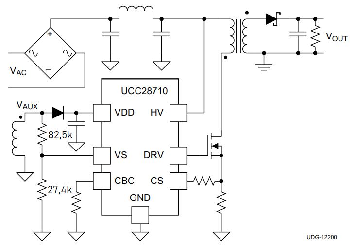
The divider resistors for vs pin are 82,5k and 27,4k respectively.

The waveform of the voltage at Vaux is below

The voltage measured at the time secondary winding reaches zero current (as shown) is about 19V.

Then with the resistor divider, the voltage at vs pin is 4,73V (> maximum threshold in the datasheet 4,7V) but there is no overvoltage protection triggered.

Moreover, the OVP function is effective just after the reset of the leakage inductance (2,2us max) and hold during the time of conduction of the secondary diode. The voltage at VS pin during that time is higher than

4,7(V), and there is no protection is triggered.

Could you explain me this conflict? 

The measure error is excluded because the probe is calibrated and auto zero.

Regards,

  • Hi Thang,

    Since your calculated 4.73V is very close to the 4.71V in the datasheet. consider the tolerance of divider resistor . the actual voltage on the VS pin maybe is lower than threshold. another possible reason is too large parasitic capacitance on VS pin . this capacitance maybe caused by long VS trace and a ground plane is under the VS pin trace and divider resistors pads .

    I recommend you to check if VS pin resistors already placed as close as the controller and make sure there is no ground plane under it.

    And you can minor increase the down side divider resistor to see if the OVP can be triggered.

    Thanks.

  • Hi Jaden,

    Thank you so much for your answer.

    I will verify your proposition.

    But there are still two things why not make sure that the capacitance is the reason.

    Firstly, there is a down slope on VS pin during the conduction of the secondary diode, and the level 4,73V is the minimum value (when the current is zero). That means the value at VSpin during that conduction could be higher than the threshold.

    Secondly, there are more than 100 switching cycles when the voltage level at VS pin may be higher than the threshold and for me there is enough time to ignore the impact of the capacitance.

    What do you think about that?

    Regards,

  • Hi Thang,

    At each switching cycle , the VS pin will been pull to negative voltage when the main mosfet turn on . that means the parasitic capacitor will be charged and discharged at every cycle . Can we talk about it after your verification test ?

    Thanks.