A related question is a question created from another question. When the related question is created, it will be automatically linked to the original question.
If you have a related question, please click the "Ask a related question" button in the top right corner. The newly created question will be automatically linked to this question.
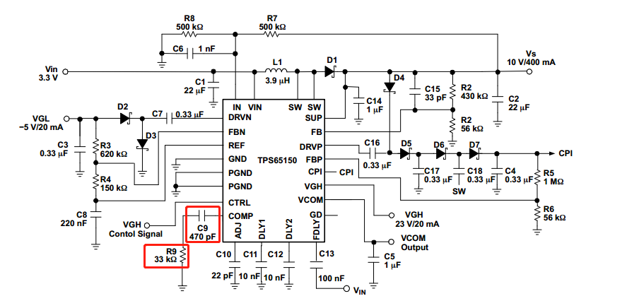
1.When VIN = 3.3 C9 = 2.2 nF R9 = 0 Ω, Ccomp & Rcomp choose like this, is OK? If this is the case, can the phase margin be greater than 45°? Friends who have actual tests can tell us. Thanks.
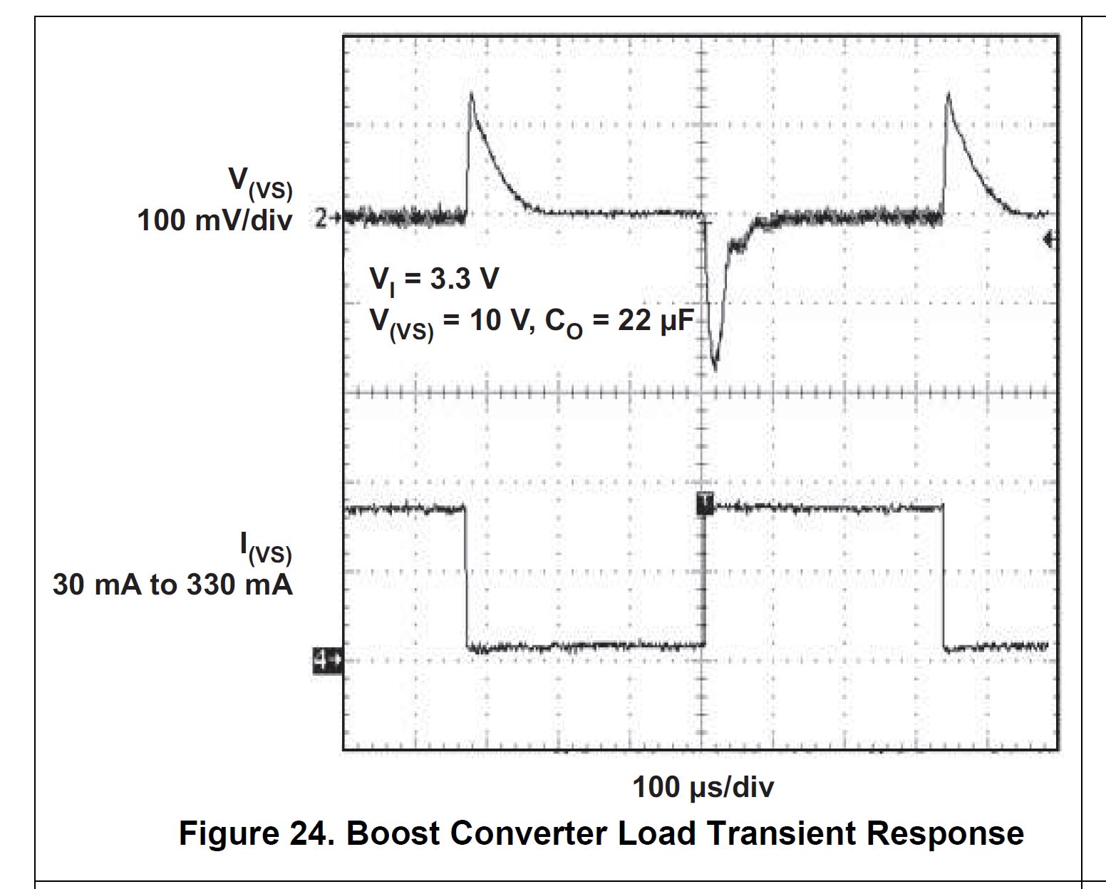
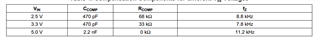
Table 1 in the datasheet lists the values for various supply inputs for these components and for Vin=3.3V, recommended values are Ccomp=470pF and Rcomp=33K. With these compensation values, Lboost=3.9uH, boost output capacitance of at least 22uF and appropriately calculated value for feedforward capacitor (C15 in the schematics you pasted above), you should get phase margin above 45 degree.
when Vin=3.3V, Ccomp & Rcomp were choosed(Ccomp=2.2nF Rcomp=0 Ω) we didn't follow recommended values(Ccomp=470pF Rcomp=33K Ω)。Since there is no loop response test facility, we want to know if there is any risk in this arrangement and if the phase margin is greater than 45°
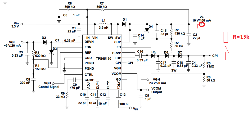
If traditional frequency reponse analysis setup is not available to you for measuring phase response, you could use a simpler method as described in the document linted below. This is only requires a load step and oscilloscope to to look at output voltage ringing.
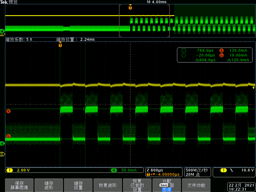
1.By your document,I mybe understand that the phase margin can simple calaculate by numbers of ringings.Whether this method is applicable to TPS65150 or not can also be calculated by the following table?
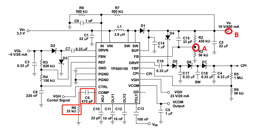
2.where is my step signal input ?Can I input the step signal from point A and test the number of ringings from point B?
1.By your document,I mybe understand that the phase margin can simple calaculate by numbers of ringings.Whether this method is applicable to TPS65150 or not can also be calculated by the following table?
2.where is my step signal input ?Can I input the step signal from point A and test the number of ringings from point B?
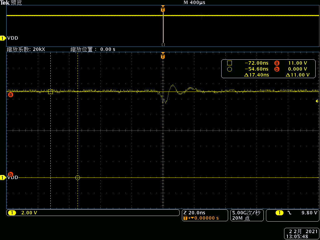
I am not sure if what you are showing is really due to load step but if it is, I see three bumps after the initial drop and that, according to the application note I sent earlier, would mean a phase margin ~35 degree. Not great but but not really bad either. If you like, you could try to reproduce the load step response shown in figure 24 of the datasheet for further confirmation.
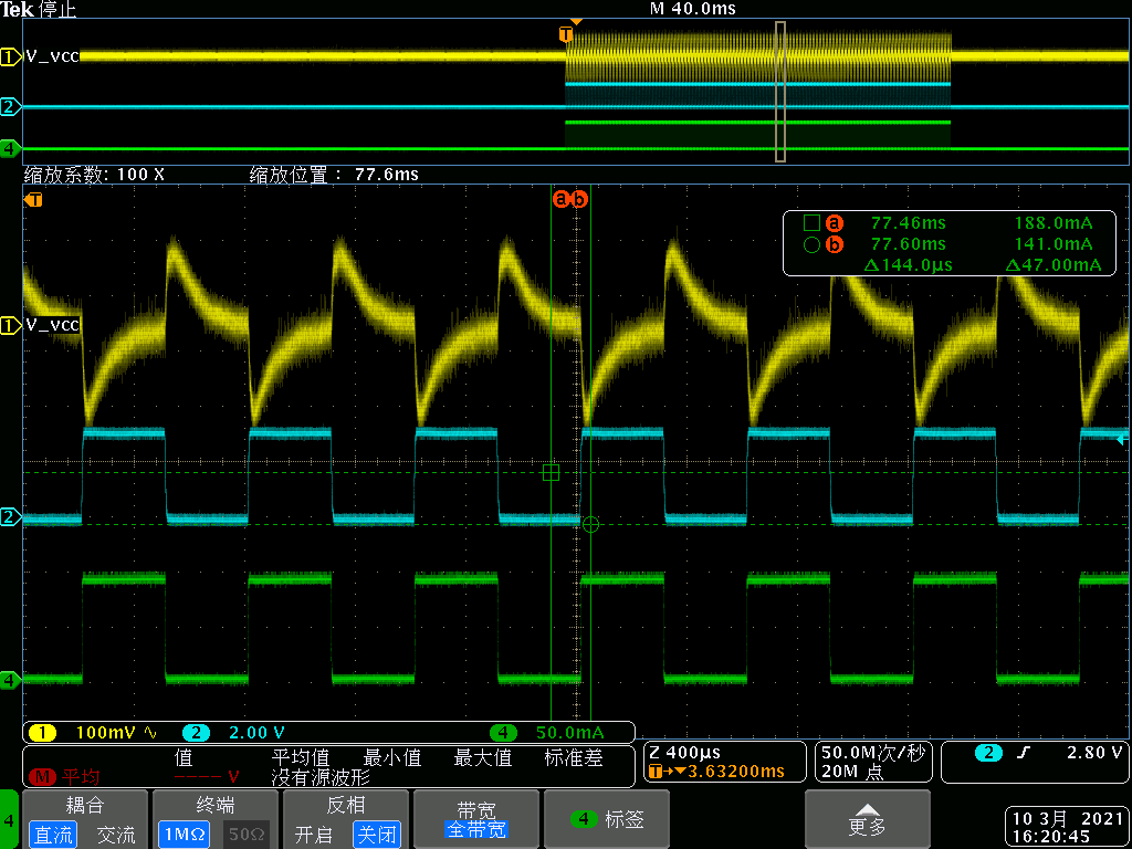
Were you successful in duplicating the results of the load step response test plot that I attached from the datasheet? I just wanted to make sure that your measurement itself is correct to take any guesswork out so I would suggest to duplicate the results of the load step response from datasheet. We normally target for phase margin of 45 degree or higher. Provided that your measurement method is correct, you can try and use the original compensation RC values for VIN of 3.3Vto see if you get higher phase margin. Also adding more capacitance at boost output normally improves phase margin.
Unfortunately, your vertical scale on channel 1 (as well as horizontal scale) is too coarse to see any ringing clearly but from what I can see, it appears to be good..
I don't see any ringing in the step response of your scope plot so this looks good to me although you could have used bigger load step (datasheet graph used a 30mA-330mA load step). This converter uses input supply voltage feed forward as part of the control loop and that is the reason for recommending different compensation for different input supply voltages.