This thread has been locked.

If you have a related question, please click the "Ask a related question" button in the top right corner. The newly created question will be automatically linked to this question.

LMG3425R030: Half-bridge GaN Lay-out

Part Number: LMG3425R030

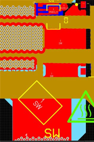
Figure 11.1 and 11.2 shows that switching node plane overlaps with power return plane. However, we know that switching node is a noisy plane and will probably make ground plane dirty below it. I have never overlapped my switching nodes in my designs so far. In the datasheet document it states that "Minimize overlap between the switch-node plane and other power and ground planes." From this quotation, I understand that overlapping has been done intentionally. The reason behind it could be that high frequency signals follows this overlapping path. If so, above what frequency does it start to hold true? If not, what is the reason behind, to some degree, overlapping switching node and ground plane ?

  • Hi,

    Thanks for the question. We do want minimum overlap between switch node and ground plane. However, there are some trade-offs in the layout. In the layout, we want the ground return to be directly underneath the part so there are maximum flux cancellation which results in minimum power loop. Wider ground return will results in smaller power loop, but larger overlap between the ground and switch node which will increase the parasitic capacitance.

    In short, we want to control the overlap to be as small as possible while maintaining a small power loop inductance. Hope this clarify your question and let us know if you have further concerns.

    Regards,

  • Could you quantify this? i.e. as a function of the overlapping area (and inter-layer thickness), there's a ratio between the loop inductance and parasitic capacitance?

  • Hi,

    It's hard to quantify, but I can show an example here. Here the yellow trace is the ground return trace and the red is the switch node. As you can see there are some overlap between them, but we controlled it to be minimum so there's a minimal additional parasitic capacitance added. 

    You can refer to our EVM layout for 1st gen or 2nd gen daughter card to get an idea. Hope this helps.

    Regards,

    Yichi Zhang