This thread has been locked.

If you have a related question, please click the "Ask a related question" button in the top right corner. The newly created question will be automatically linked to this question.

TPS22917: TPS22917 sequencing TUSB1210 on Zynq 7000 design

Part Number: TPS22917
Other Parts Discussed in Thread: TUSB1210, TPS22953, TPS22954, TPS22951

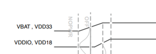
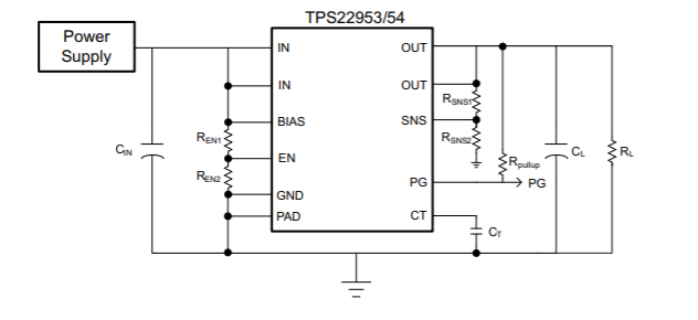
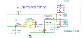
I am using the TUSB1210 with a Zynq XC7Z010. There is good information on sequencing the 1.8V rail for VDD18 and VDDIO after VBAT/VDD33, which is the opposite of what the Zynq system provides. I tried using the TPS22917, but it appears that the load switch is oscillating on and off. When I short Pin1 and Pin6 together, the TUSB1210 is able to start up with no problem. Is there a recommended load switch design for the TUSB1210? Also, it seems like the TPS22917 does not have a well-defined turn on/off point or hysteresis, so probably I need a part that has a well-defined turn-on voltage? The TPS22917 allows the Output to come on before the 3.3V rail is well established because I didn't use a resistor-divider.

Load switch schematic

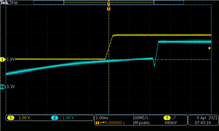
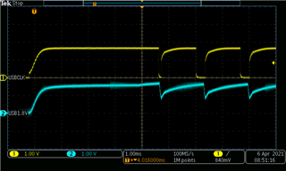
With TPS22917 in place:

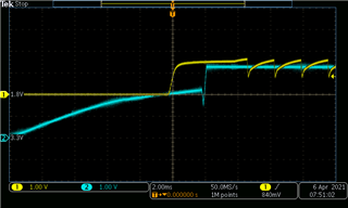
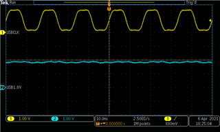
With TPS22917 Pin1 and Pin6 shorted:

TPS22917 delays the USB_1.8V but not enough, because the 3.3V rail rises slowly compared to 1.8V, and there is no resistor-divider and no tightly controlled turn-on voltage.:

Before load switch

After load switch

  • Hi Paul,

    TPS22917 is meant to be used in DC applications. Im not sure what the goal of TPS22917 is in this case and I think you may benefit more from a signal switch instead of a power switch. The V_il and V_il of TPS22917 are 0.35V and 1V and operation between this voltage on the ON pin is not recommended. 

    We also do not recommend the use of the device with input voltages less than 1V. I also noticed that the ON pin is tied high and thus, I am not sure how you are getting the device to turn on and off apart from oscillating VIN which is not recommended. 

  • Hi Shreyas,

    I would like the load switch to provide the correct sequencing. It was my mistake not to include the resistor-divider on the ON pin, but it also seems like an IC designed for this is more likely to have well-defined voltages and hysteresis for the ON input. Should this be moved over to the TUSB1210 forum, since I am really asking for a recommended design patter to be applied to that IC?

  • Hi Paul,

    I believe there might be something in the signal switches portfolio but I could be mistaken. 

    Please take a look at the signal switch offerings here: https://www.ti.com/switches-multiplexers/analog/overview.html

    If a switch seems to fit your bill, then please post a new question with that device tagged.

    I think another option to get support quicker on this request may be to repost the question but only mention the TUSB device  Something along the lines of "TUSB signal sequencing"

    I could also move this thread but at this time, I am not sure if the signal switch forum will be most helpful compared to the TUSB forum. 

    For now, I will close this thread but in case you would like me to move this once you have taken a look at the signal switch portfolio, let me know.

  • Hi Shreyas,

    This is for power sequencing, not signal control, as shown in the schematic. The top scope capture is just showing that the USB_1.8V gets pulled down repeatedly. The second capture is showing that I have a valid clock signal as a way to indicate that the TUSB1210 is working once I bypass the TPS22917. Is there a recommended load switch for this sequencing?

    Thanks,

    Paul

  • Hi Paul,

    What is your goal here and what are the operating conditions?

  • My goal is to meet the recommended power-up sequence for the TUSB1210. The operating conditions are shown in the schematic. The TUSB1210 receives a 1.8V and 3.3V power from the rails on the board. My big concern is the hiccup behavior seen with the TPS22917. If I just pick a different load switch, how do I avoid this problem again? I would be much more comfortable if there is power sequencing circuit that TI can recommend.

    Power sequencing on the board: 


    Power sequencing recommended by the TUSB1210 datasheet (timing is not critical).

    An E2E post which also describes the recommended sequencing for TUSB1210: https://e2e.ti.com/support/interface/f/interface-forum/816141/tusb1210-power-on-sequence

  • Hi Paul,

    Thanks for the background. From my understanding, you need to power up the 3.3V signal before powering the 1.8V.

    Unfortunately, you are in a situation where since 3.3V rises slowly, TPS22917 does not delay the turn on time enough for successful power up and the only signal that you are working with is the 3.3V. I think even if you use a tight Vih, Vil device you will run into this as the 3.3V rises quite slow.

    I think a potential workaround is to use two switches in the following setup:

    1. Use TPS22953/TPS22954/TPS22951 (depending on your preference) on the 3.3V rail. For this device you can use an pull down resistor on EN and connect VIN, VBIAS and EN to the 3.3V signal. As the 3.3V signal rises, this will turn on the device and the output of this device will send 3.3V to the MCU.

    2. Setup the VSNS pin on TPS2295x in such a way that it pulls PG high(PG connected to VOUT) only after VOUT has risen to lets say 3.2V. This is done by way of a resistor divider on the output. Here is the setup:

    3. Connect this PG pin to the EN pin of TPS22917. Based on the CT capacitance for TPS22917 you can set the delay and rise time as you need.

    I think TPS22917 can be switched out with other load switches if you do not require all the features of TPS22917 but I think with the TPS22953 on the 3.3V rail you will be able to build a "voltage relay" of sorts with two load switches.