This thread has been locked.

If you have a related question, please click the "Ask a related question" button in the top right corner. The newly created question will be automatically linked to this question.

UCC27712: Inquiry about HS pin Min voltage of UCC27712

Part Number: UCC27712

Hi, TI expert.

I have a question about Min voltage (-voltage) of HS pin of UCC27712.

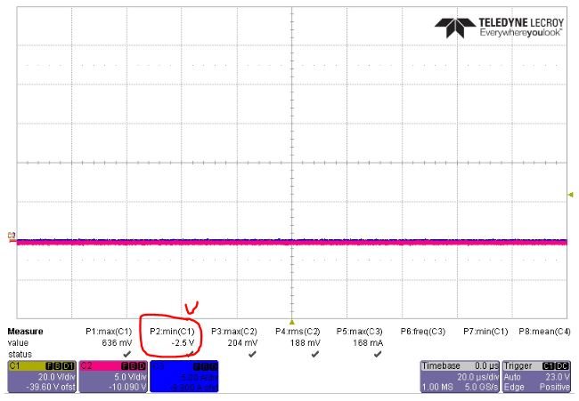
If you look at the datasheet, the Min voltage of HS pin is -11V in operating condition.

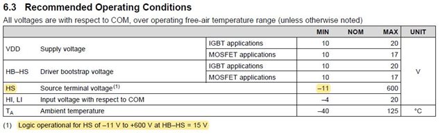
Q1)  However, when measuring the HS pin during normal operation, Min (-11.3V) was measured. (Refer to Waveform-1)

In normal operation, HS-HB: 14.63V is measured as 15V under, but it is out of -11V, the Min spec of HB pin.

Is there any problem with the operation?

Q2)  Also, if HS pin is measured during Peak Load operation, Min (-14.3V) is measured. (Refer to Waveform-2)

The HS-HB voltage is also 19.69V.  Is there a problem with the operation?

[Waveform-1,  HS pin Min voltage during Normal operation : -11.3V  (CH1 : HS pin , CH2 : HS-HB , CH3 : Output current) ]

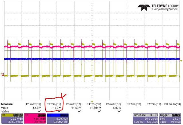
[ Waveform-2,  HS pin Min voltage during peak load operation : -14.3V  (CH1 : HS pin , CH2 : HS-HB , CH3 : Output current) ]

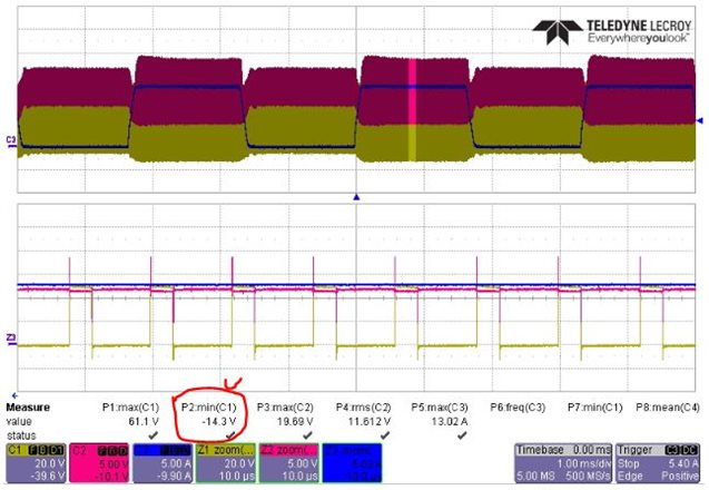
In the basic state of the scope without measuring any terminal, -2.5V is output. (Refer to Waveform-3)

[ Waveform-3, In the basic state of the scope without measuring any terminal ]

Please check.

Thank you.

  • Hello,

    Thanks for reaching out.

    We're reviewing the details of the problem and will get back to you promptly.

    THanks.

    -Mamadou  

  • Hello Grady,

    Thank you for the detailed information in your post. The datasheet lists in the table HS negative voltage of -11V with a VDD of 15V. In the datasheet section 7.4.4 there is a more detailed description of the operation and Figure 43 shows a curve for HS negative voltage Vs time.

    If there is a negative DC voltage on HS which results in HB - COM being < 4V, the HO level shifter cannot recognize the signal and will not react to the edge, which would be a turn on edge if HS is low.

    In almost any application, when there is an HS negative spike it is when HO is turned off, and later LO is turned on and you just need to ensure HO maintains the off state and LO is on.

    The curve in Figure 43 shows the negative HS pulses where the HO output will maintain the correct state but may not react to an HI input if HB-Com is < 4V.

    The waveforms you show look to be OK for the operation. Just make sure the HS negative voltage and time duration is within the curve in Figure 43.

    Confirm if this addresses your question, or you can post additional questions on this thread.

    Regards,