- Ask a related questionWhat is a related question?A related question is a question created from another question. When the related question is created, it will be automatically linked to the original question.
This thread has been locked.
If you have a related question, please click the "Ask a related question" button in the top right corner. The newly created question will be automatically linked to this question.
Hello,
I am trying to implement a CC Buck and am using this application note as my guideline http://www.ti.com/lit/an/snva829/snva829.pdf. My input is 57 volts and I want the output to give constant 6 A over a 20-45V range at 300 kHz. I used the provided excel file to size my components and the complete circuit is given below. The switches are CSD19537Q3 http://www.ti.com/product/CSD19537Q3 and the inductor is Coilcraft XAL1510-333MEB https://www.coilcraft.com/xal1510.cfm
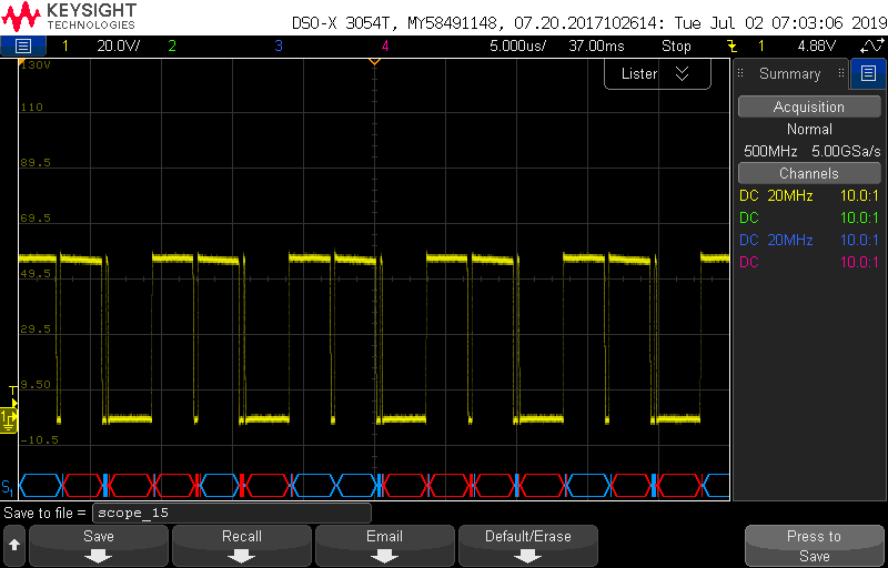
I am using an electronic load in CR mode as my load right now. When the load resistance is >14 Ohms the converter gives a stable CV, but the switch node looks odd (see attached). When the load resistance drops below 14 Ohms the converter becomes unstable, presumably because it begins to enter CC mode and something is wrong. Any insight into what I could be doing wrong would appreciated and I can provide additional probe images if needed.
Thanks
1033.lm(2)5117_quick_start_hv_calculator V1.5.xls
Hello Jason,
Please exactly follow the design approach given in the application note.
For your circuit design you will yield a CMave output voltage of 1.2V. You have to have a FB resistor divider network from CM to Gnd with the divider point connected to the FB node. Set Rfbb to 10k (bottom FB resistor) and a Rfbt calculates to 5k (top FB resistor). A good starting point is using the compensation components shown in the application note.
Hope this helps?
Do you mean the schematic given in Figure 3 of the application? That is pretty much where most of my circuit came from.
I have the divider from CM to FB to GND. The top resistor is 3.7k (same as the app note) and the bottom is 10k (same as app note). The voltage shunt regulator I am using has a different reference voltage (2.5 vs 1.25 in app), so those resistors are slightly different, but all in all its mostly overlap.
Sorry Jason,
You are right, you do have the Resistors in the correct place. Change the top FB resistor from 3.7k to 5k.
As for the RC (R9/C8) components from FB to Comp, please use a 1k and 100nF as a starting point. This should stabilize the loop?
Hope this helps?
Thanks Jason,
before I scrutinize the layout can you try one last thing for me. Please can you refer to Fig 3 in the app note. Note there is a RC (R11 and C19). Can you please add and recheck.Make R11 = 1k and C19 = 10nF.
FYI, you are in CV mode with Rload = 10ohms and no where near the transition point from CV to CC. this will happen at 6A Iout... which is Rload ~6ohms.
Hope this helps?
Since R11 was a short and C19 was a "Do not populate"(?) I didn't include it in my layout. I can add C19 to the board across the pins, but can't make R11 without digging up the traces.
Makes sense on the CC/CV boundary, however, I am getting the oscillatory unstable behavior if Rload is 12 or 6 Ohms.
Hello Jason,
Instability is typically caused by the following,
1. Compensation - Ruled out if with Rload<6ohms still unstable with Rcomp and Ccomp = 1k/100nF
2. Input filter instability - Even if you do not have a filter at vin, but you are using long input cables with parasitic inductance as a result. Will need to parallel damp. Suggest a bulk input cap of at least 4x the cin ceramic being used. Suggest 10x if you can and an ESR of ~0.5ohms or greater.
3. Layout. this is the most likey cause if 1 is completely ruled out with Rcomp/Ccomp and r11 and C19.
From the layout you posted it looks as though the current sense input is not ideal, it looks like you ground CSG to the DAP? Also It looks like the Analog Gnd pour is non ideal?
Please refer to the attached and follow the guidelines closely there in.
Hope this helps?
Pin 14 (PGND) is tied to the DAP while I differentially ran my Rsense wires.
I added 300 uF (3x100uF) electrlytics to the input, but am still getting instability.
I don't have the ability to add r11 and c19, so if that is the issue Ill have to remake the board.
If I do remake the board, what should I change about my AGND? It is currently a star configuration and the pour has minimal cutouts.
Hello Jason,
I suggest you follow closely the document I sent, tying all small signal components back to a AGnd Polygon pour that then route back to the Agnd pin of device, using a low Z path (as depicted in PDF).
Please feel free to open another thread in the forum, once you have completed the layout closely matching what I sent previously. We can provide additional help.
Hope this helps?
If I am understanding this correctly, the ground tie connection should be at the AGND pin and the DAP?
Hello Jason,
Correct, Tie all small signal components directly to Agnd pin and then stitch Agnd pin to the DAP by the AGnd pin.
Hope this helps?