Other Parts Discussed in Thread: BQ76930, TIDA-00449, ISO1540
Good day,
I just finished my schematic for a 9S Li-Ion BMS, and would like to ask for help if there's something wrong/missing in my schematic before I proceed to the PCB layout.
Some info:
-I used http://www.ti.com/lit/df/tidr773/tidr773.pdf as reference
-I'm only going to use 9 batteries in series, to be used for an E-Bike
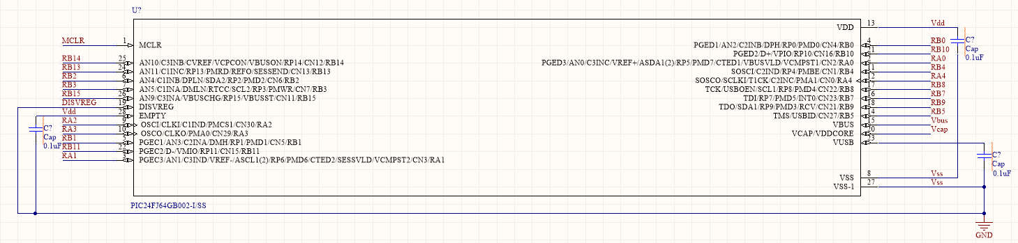
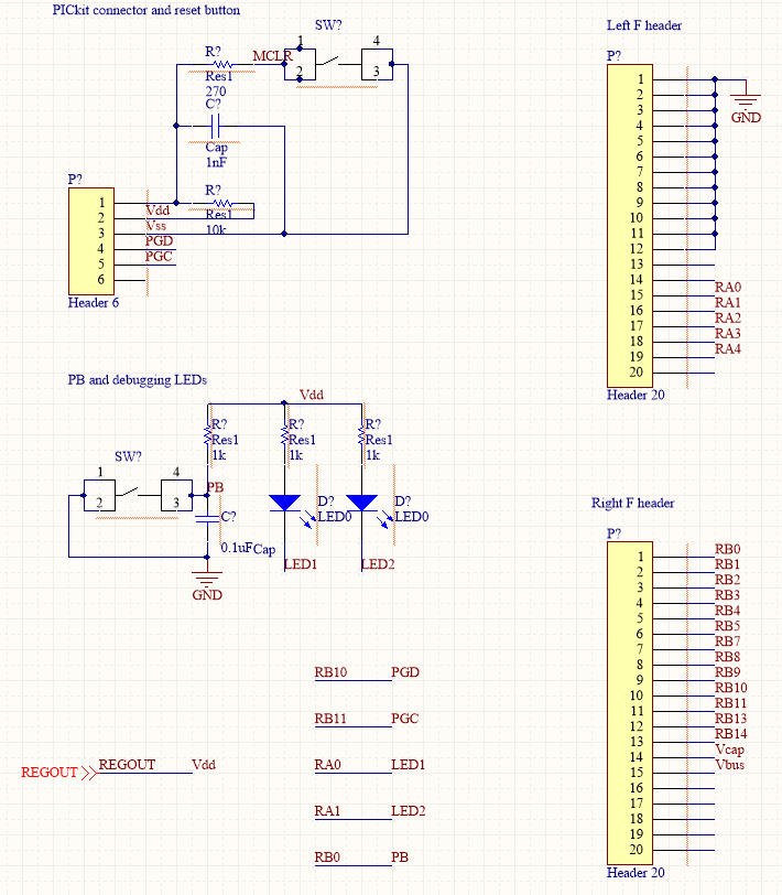
-I'm using the PIC24 as my microcontroller
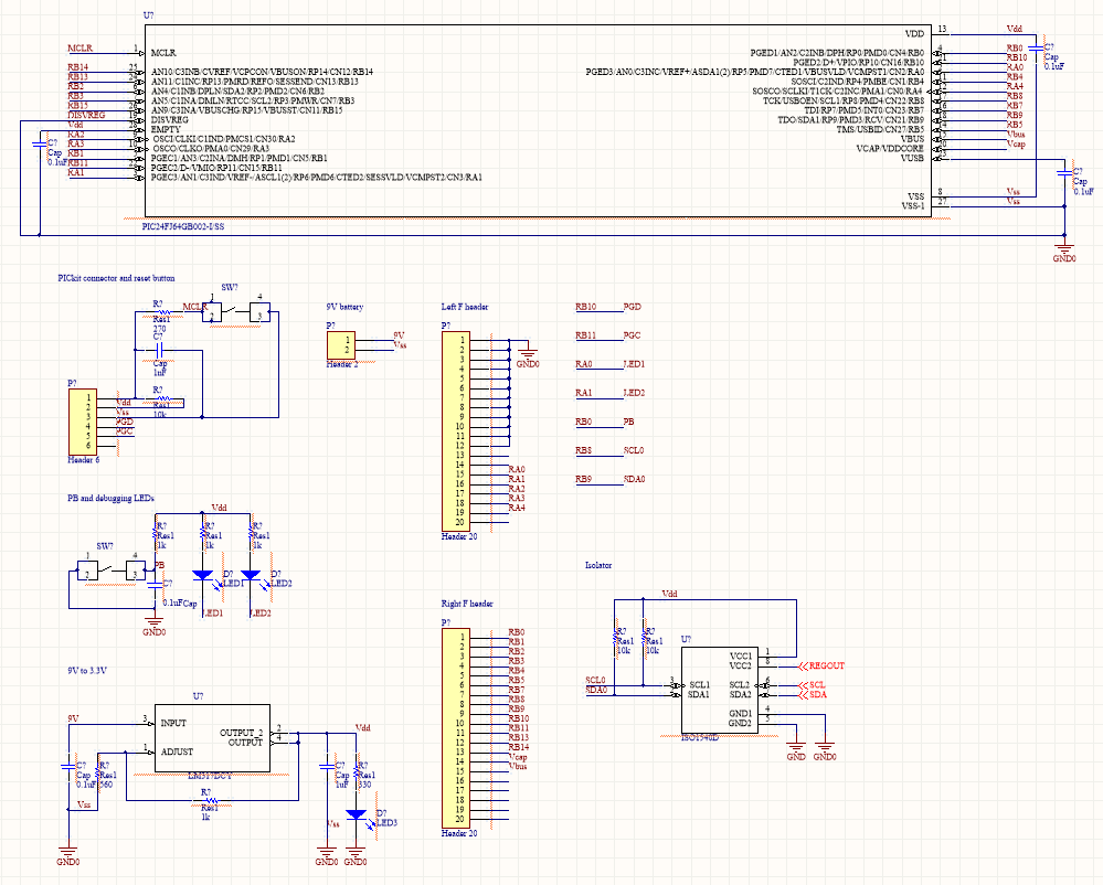
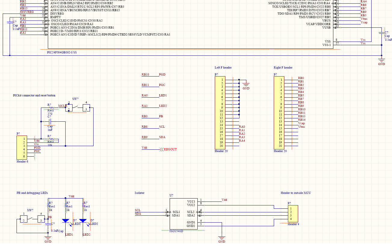
Sheet 1: Microcontroller
Sheet 1-complete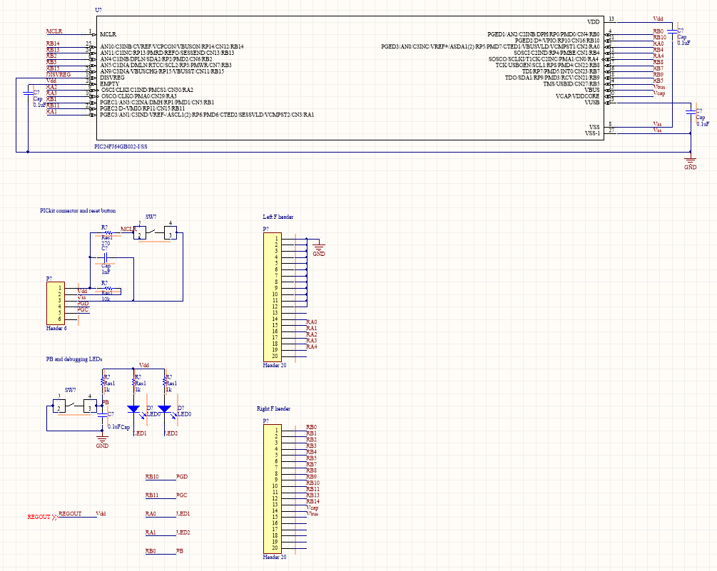
Sheet1-1
Sheet 1-2
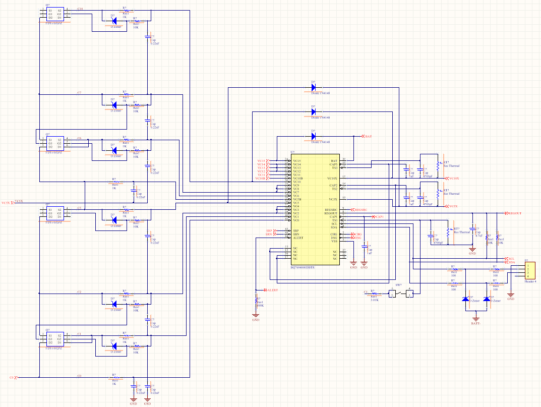
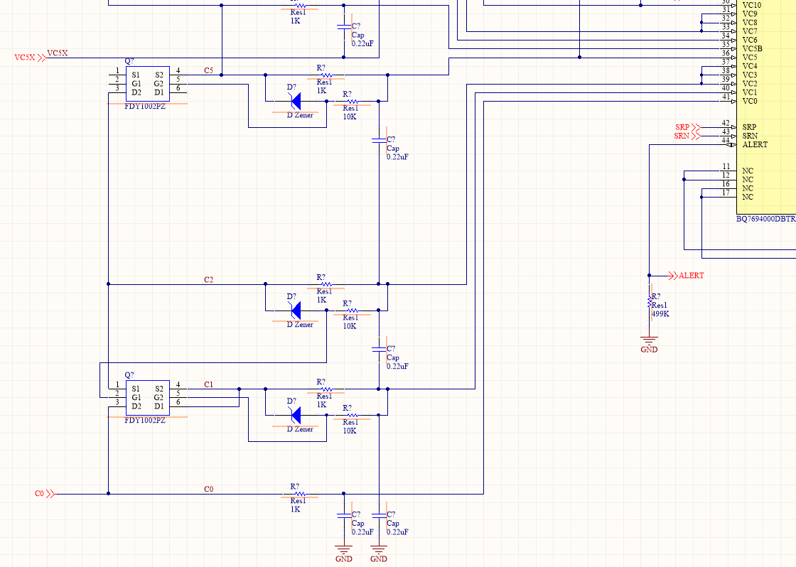
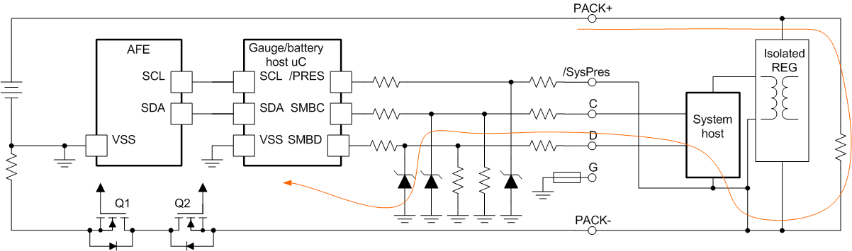
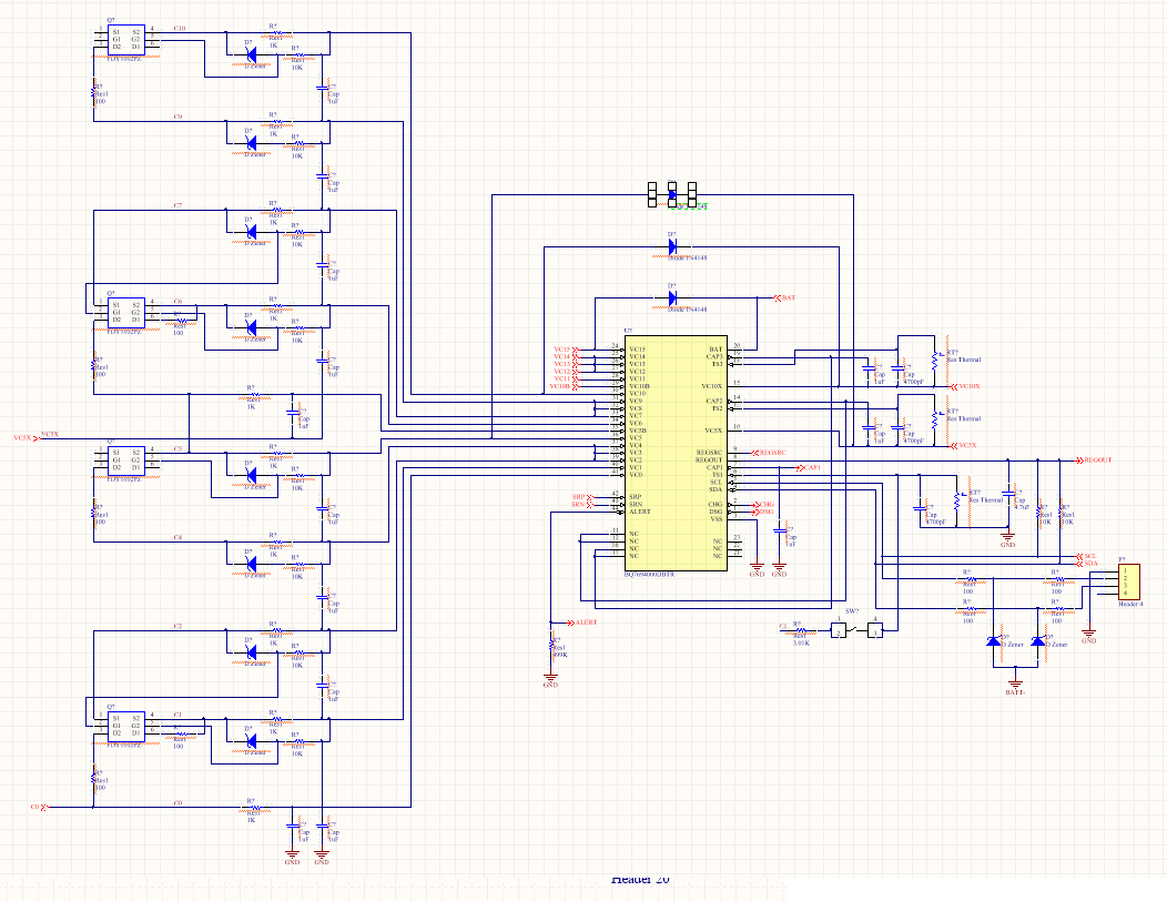
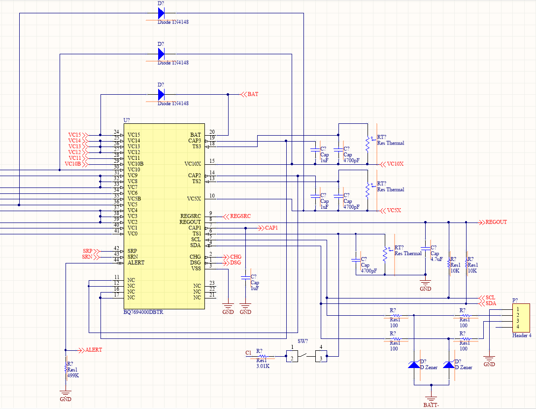
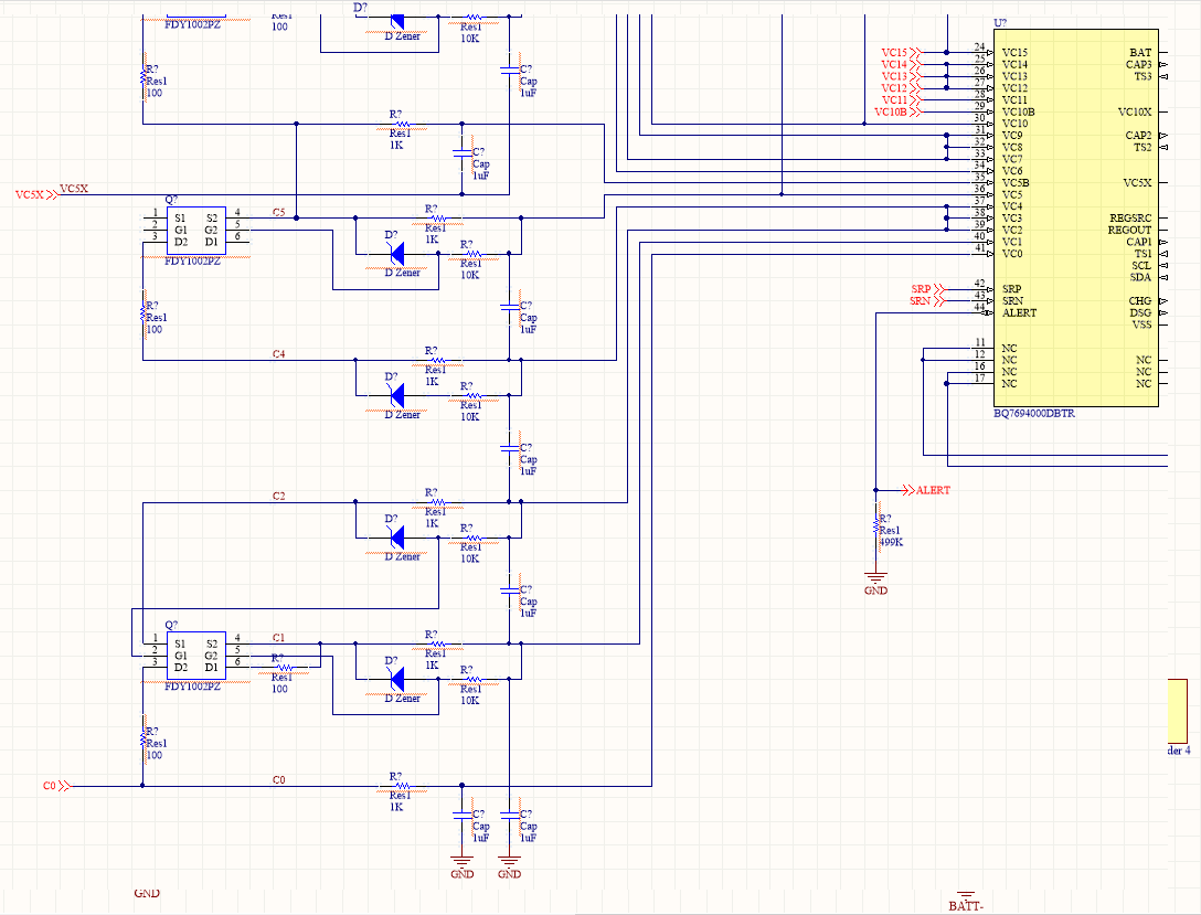
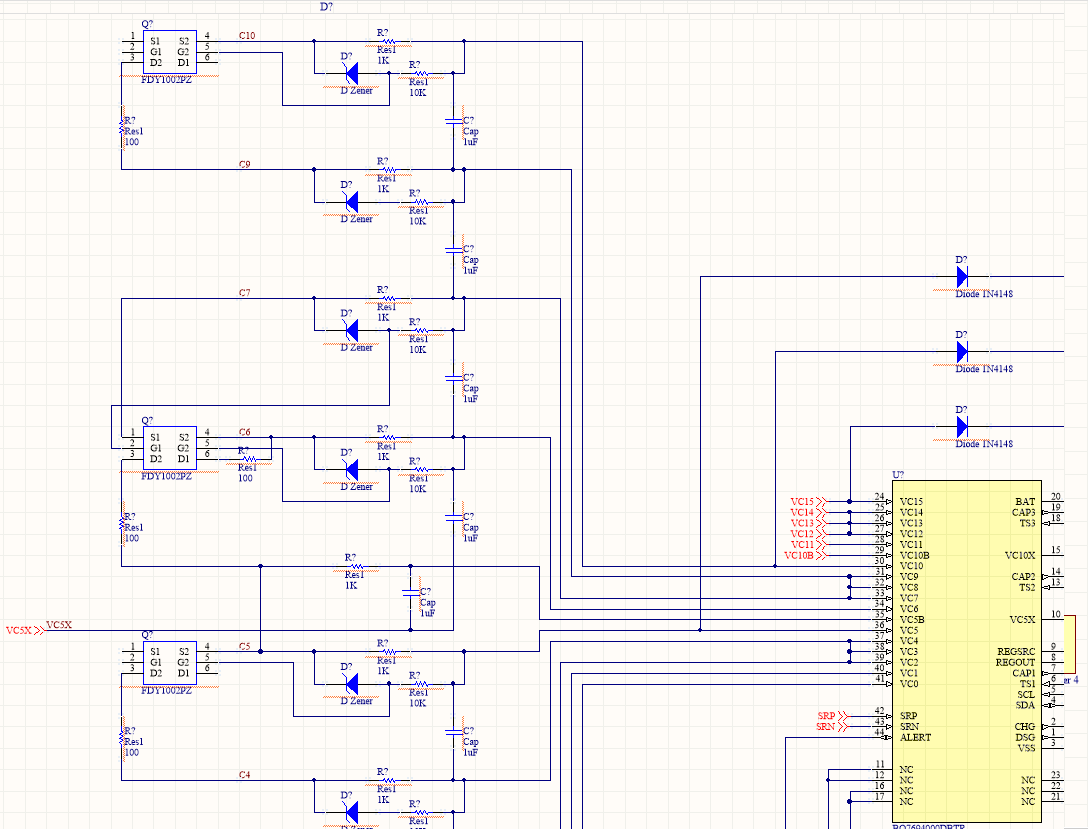
Sheet 2: AFE lower and power out
Sheet 2-complete
Sheet 2-1
Sheet 2-2
Sheet 2-3
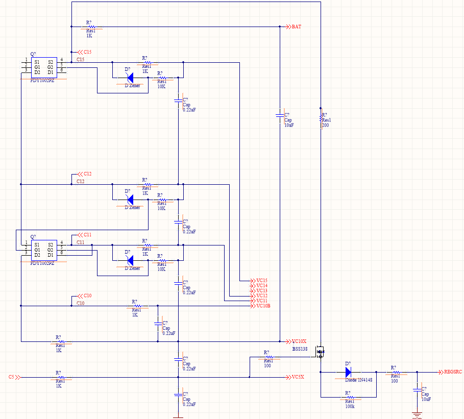
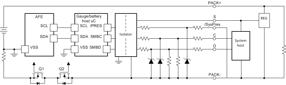
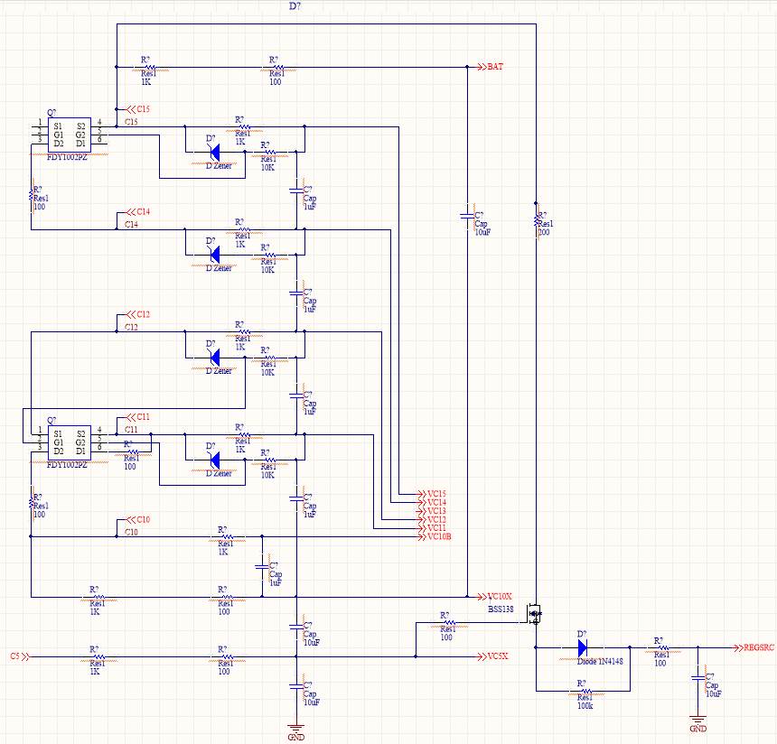
Sheet 3: AFE top and power in
Sheet 3-complete
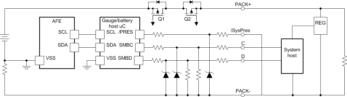
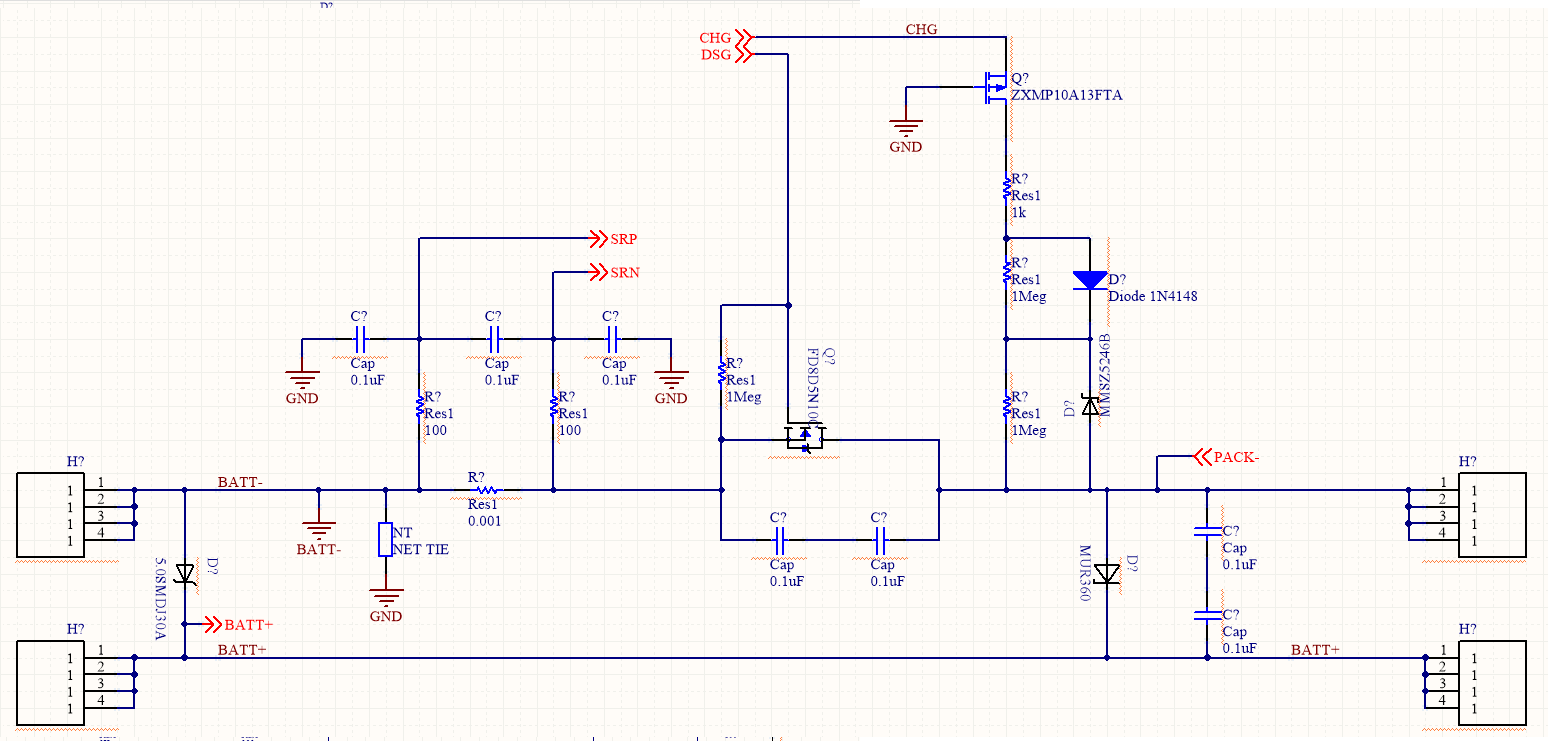
Sheet 4: Power FETs
Sheet 4-complete
Thank you very much,
Robert