This thread has been locked.

If you have a related question, please click the "Ask a related question" button in the top right corner. The newly created question will be automatically linked to this question.

TPS53353: DESIGN REVIEW

Part Number: TPS53353
Other Parts Discussed in Thread: TPS62130A, , TPS53355

We have designed a server motherboard based on Intel's purely platform. The power controllers were used in the design are of TI and we took the help of webench for the reference design. We have been facing power issues while testing those boards. we are planning for the V2.0 release of the design. Before going for that step, we want our design to be reviewed by TI.

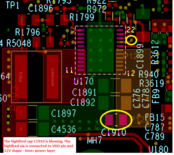
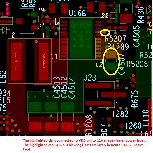
During the bring up some input capacitors were blown. (Refdes: C1874, C1910). - schematic is attached

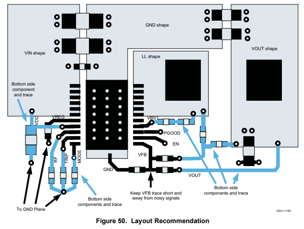
Also please suggest the Input filter or EMI filter circuit as we did not implement such a filter circuit at any stage.

Please let me know if anything is needed

Rudra2.0_TIPower.pdf

  • Hi Neha,

    I have attached the schematic and layout checklist and calculator for the TPS5335x family of devices. Please fill these out and let me know if you have any further questions.

    Best regards,

    Layne JTPS5335x_Calculator_Checklist.xlsx

  • Thank you Layne.

    I am going through checklist. and we also have TPS62130A in our board.

    The same capacitors are blowing up in our board. what might be the reason, can you help in this?

    Can you also provide some inputs to design input filter?.

  • Hi Neha

        Can you please let us know which capacitors are blowing (input or output)? Please send us the voltages that are being applied to the capacitors and the voltage ratings of the caps being used (preferrably the part numbers).

    Regards,

    Gerold

  • The original post states that input capacitors were blown.

    The specific reference designators are the 4.7uF VDD bypass capacitors for the TPS53353 converters.  they are directly connected to the 12V VIN and there appears to be only minimal VIN to GND bypassing at the input to each of the converters.

  • Hi Gerold,

    Input capacitors are blowing refdes are C1910, C4040, C1874

    The voltage applied to caps is 12V


    CAP, CER, 4.7uF, 25V, 10%, X5R, 0805 : Taiyo Yuden Corporation : TMK212BJ475MG-T

  •  

    Can you please share the WeBench output files in PDF format for these designs?

    Also, if you have some graphics that show the placement of the VIN bypass capacitors relative to the TPS53353 converters and they ground connections back to the thermal pad of the TPS53353 controller, that will help us offer suggestions.

    The devices that are identified as blowing up are the 4.7uF VDD to ground bypass capacitors.  As 25V ceramic capacitors, it is unlikely that they are being damaged by over-voltage, but the input RMS ripple of a Synchronous BUCK converter can be very high, and these schematics show only 1 or 2 VIN to GND bypass capacitors carrying 2-3A of RMS current each.  If the primary 22uF or 47uF capacitors are not well bypassed, or are located away from the TPS53353 converter, the 4.7uF VDD bypass capacitor could be trying to carry the majority of this RMS current and failing.

    As a general practice, it would be preferred to separate the VIN and VDD inputs with a 10-ohm resistor for a 12V input in order to keep VIN switching currents out of the VDD bypass capacitor.  It is also preferred for the VIN bypass capacitors to have a tight loop with multiple vias if changing layers, from the VIN IC pins through the device to its thermal pad, back to the ground of the VIN bypass pins and then from the VIN terminal of the capacitors back to the IC VIN pins.

  • Hi peter,

    I have also probed the capacitors with trigger mode during power on - multiple times. The voltage across the capacitors are not going beyond 12.5V with 12V nominal voltage input.

    I am attaching the layout snapshots of three supplies with C1910, C4040, C1874 as VDD capacitors.

    Also I am attaching Webench reference pdf files   p3v3_aux.pdf

  • C1910 - P3V3

    C4040 - P3V3_AUX

    c1874 - P1V0

    P3V3.pdfP1V0_PCH_AUX.pdf

  • Hi Neha,

        It looks like the VDD capacitors are quite far away from the pin. Have you tried getting an EVM board and changing the BOM components on the board to your BOM components? If so, that could give an indication that the layout is an issue.

    Have you tried running simulations with your BOM?

    Regards,

    Gerold

  • Hi Gerold

    The maximum air gap between the cap and ic pins is ~350mil.

    The reference layout in the datasheet suggests that the VDD bypass cap to be placed on the bottom layer and it has a different trace to connect to 12V. In our case Input caps and VDD bypass caps are sharing the same shape (top) and in some cases, this VDD bypass cap is closer to IC than the Input caps.

    Is there any chance that VDD bypass cap is taking more input ripple and blowing because they are closer?

    I have not done the simulations for our BOM. only input and VDD caps are different from webence ref design as they were obsolete. 

    Thanks & Regards,

    Neha

  • Hi Neha,

         The VDD pin should have a dedicated cap that is closer to the IC. In your case the VDD cap is far away from the IC and essentially the pin does not have any bypass cap now. This might be creating too much ripple and causing the capacitor to blow.

    Can you try putting a higher current rating capacitor for the VDD caps - to see if those can withstand the ripple current?

    What happens to the converter after the caps blow up? Is the converter shutting down?

    Anyway, this might be needing a new layout. Are you considering a board respin at this point?

    regards,

    Gerold

  • After blowing , the input impedance ( 12V) dropping to 0 ohms, so the hot swap controller on the board is shutting down the all the supplies. But the supply is working fine even after removal of that cap.

    Will try with 50V cap and let you know.

    Yes, we are going for the respin by this month end. So ready to change the necessary layout changes.  Suggest if any else seems wrong to you in the layout.

    Thanks & Regards,

    Neha

  • Hi Neha,

        Can you please complete the schematic/layout checklist that we sent you? This captures all the key points that need to be addressed. Once you complete the checklist, you can send it to us and we can let you know if there is any feedback.

    Regards,

    Gerold

  • Hi Gerold,

    I am going through the checklist. I have some doubts in the checklist:

    1. Iout load transient step current is not calculated in our design anywhere before, I am considering 50% of tha maximum required. Is that ok?

    2. In checklist Cin has multiple capacitors- I have followed webench and webench did not recommend any of these.

    Add multiple (preferable 6) 2.2nF-10nF 0402 minimum 25V input capacitor from PVIN to PGND to minimize high-frequency ringing energy
    Add a 1x1uF capacitor to the input capacitor bank.

    I will complete the checklist and send you the same asap.

    Thank you

    Regards,

    Neha

  • Hi Neha

         The load transient step size depends on your application. What do you think will your load current range. For example if you think your load Iout max =20A (as an example) would step from 10A to 20A, then your step size is 50%. If you think it would go from 0A to 20A , then your step size is 100%.

    100% is the worst case - so, if you are not sure, it is ok to use 100%. It really depends on your application.

    Regarding the checklist recommendation, these are best practices - we will be adding some of these best practices into WEBENCH soon. The best practices might help you get a better design in terms of performance (low ripple etc.) on top of the existing WEBENCH design.

    regards,

    Gerold

  • Hi Gerold,

    Thank you for your reply.

    I have completed the checklist by considering 100% load step current.

    The items which are completely followed, I have changed the status to completed for those. The rest were remain kept open. 

    Please find the attached checklists

    Thanks & Regards,

    Neha

    TPS5335x_Calculator_Checklist - P5V0_AUX.xlsxTPS5335x_Calculator_Checklist - P3V3.xlsxTPS5335x_Calculator_Checklist - P3V3_AUX.xlsxTPS5335x_Calculator_Checklist - P1V0_PCH_AUX.xlsxTPS5335x_Calculator_Checklist - P1V05_PCH_AUX.xlsx

  • Hi Neha

         Thanks for using WEBENCH. There are cases in the checklist where it is recommended to use a high frequency cap etc. Please do that - as it might be something better..

    Also for VREG LDO, please follow the checklist recommendation of 1uF - just to be safe.

    Any specific questions that you have?

    Regards,

    Gerold

  • Hi Gerold,

    Thank you for going through the checklist.

    Could you just summarize the changes we need to do before going for re-spin? 

    Please add your points to this summary:

    1. Addition of multiple ( preferably 6) high-frequency VIN caps (2.2nF - 10nF 0402) - schematic checklist D23

    2. Changing of VREG cap from 300nF to 1uF 25V 0401(min)

    And what might be the reason for VDD capacitor blowing up -?

    From our previous conversation, I understand that the Placement of VDD cap and VDD, VIN were connected to 12V trough the same shape were the issues. You have suggested that Place VDD cap close to VDD pin and separate shape ( VIN and VDD shape different), also isolate VDD 12V and Vin 12V by a 10-ohm series resistor. Should we do this change also?

    Thanks & Regards,

    Neha

  • Hi Neha

       The cause the VDD cap blowing is mostly the layout. I have not checked if the list that you have mentioned covers all the items in the checklist.

    Please ensure that all items in the checklist both schematic and layout are covered.

    Regards,

    Gerold

  • Hi Gerold,

    Yes, The VDD caps placement is violated from the checklist. Surely we will implement the checklist items in the next spin.

    Apart from the checklist items, Do we need to isolate  VDD 12V and Input 12V  by 10 Ohm?

    Thanks & Regards,

    Neha

  •  

    The reason the 4.7uF VDD bypass capacitor in your design was failing is most likely due to excessive layout parasitics between this 4.7uF bypass capacitance and the primary VIN to ground bypass capacitance causing the 4.7uF capacitor to handle the majority of the RMS ripple current flowing into the VIN pins.  The input current of a BUCK regulator has very high RMS ripple current.  Normally, this input RMS current is spread between multiple parallel input capacitors to distribute the thermal stress across multiple devices, but this AC ripple current sharing is subject to the effects of the parasitic inductance between the capacitors.

    In your layouts, especially the U168, the 4.7uF capacitor is located closest to the IC while the 22uF bypass capacitors are located further away.  That arrangement will drive most of the high RMS current through the smaller 4.7uF bypass capacitor instead of the 22uF capacitors, which will likely cause them to heat-up and fail.

    Separating the VDD bypass capacitor from VIN with a 10-ohm resistor will certainly help reduce the RMS stress on the VDD bypass capacitor, but making sure the 10uF and 22uF bypass capacitors from VIN to GND are located as close to the TPS53355 as design rules allow, have similar parasitic impedances and sufficient RMS ripple current handling will help equally distribute their current handling.