This thread has been locked.

If you have a related question, please click the "Ask a related question" button in the top right corner. The newly created question will be automatically linked to this question.

BQ76952: Problem faced while testing Cell Balancing feature of BQ76952

Part Number: BQ76952
Other Parts Discussed in Thread: BQSTUDIO, BQ7718, TIDA-010030, BQ34Z100-G1

Hello TI Team,

 Problem faced while testing CELL Balancing feature, 

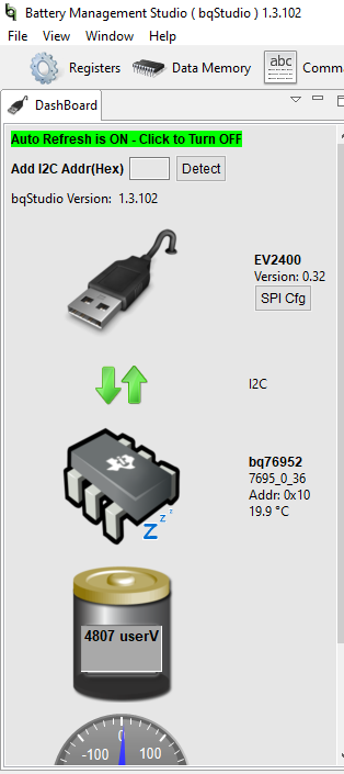
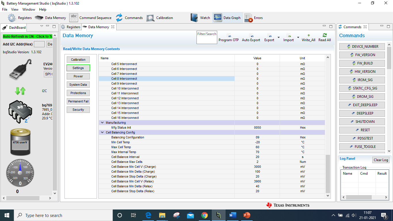
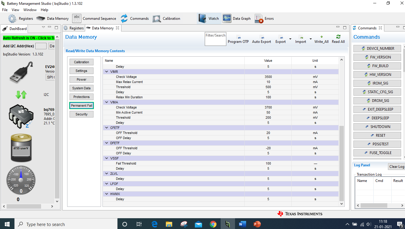
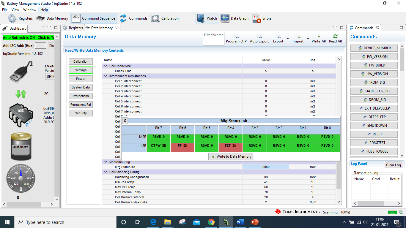
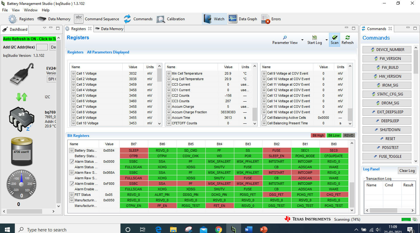
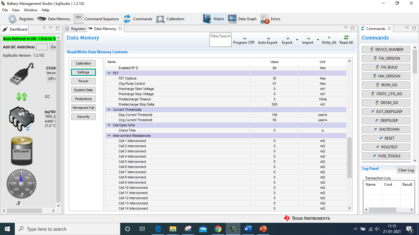
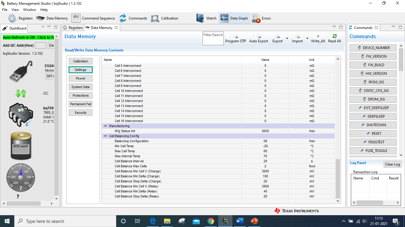
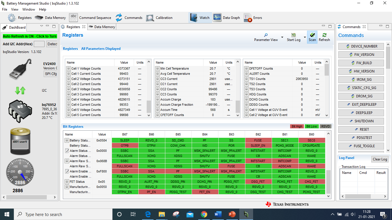
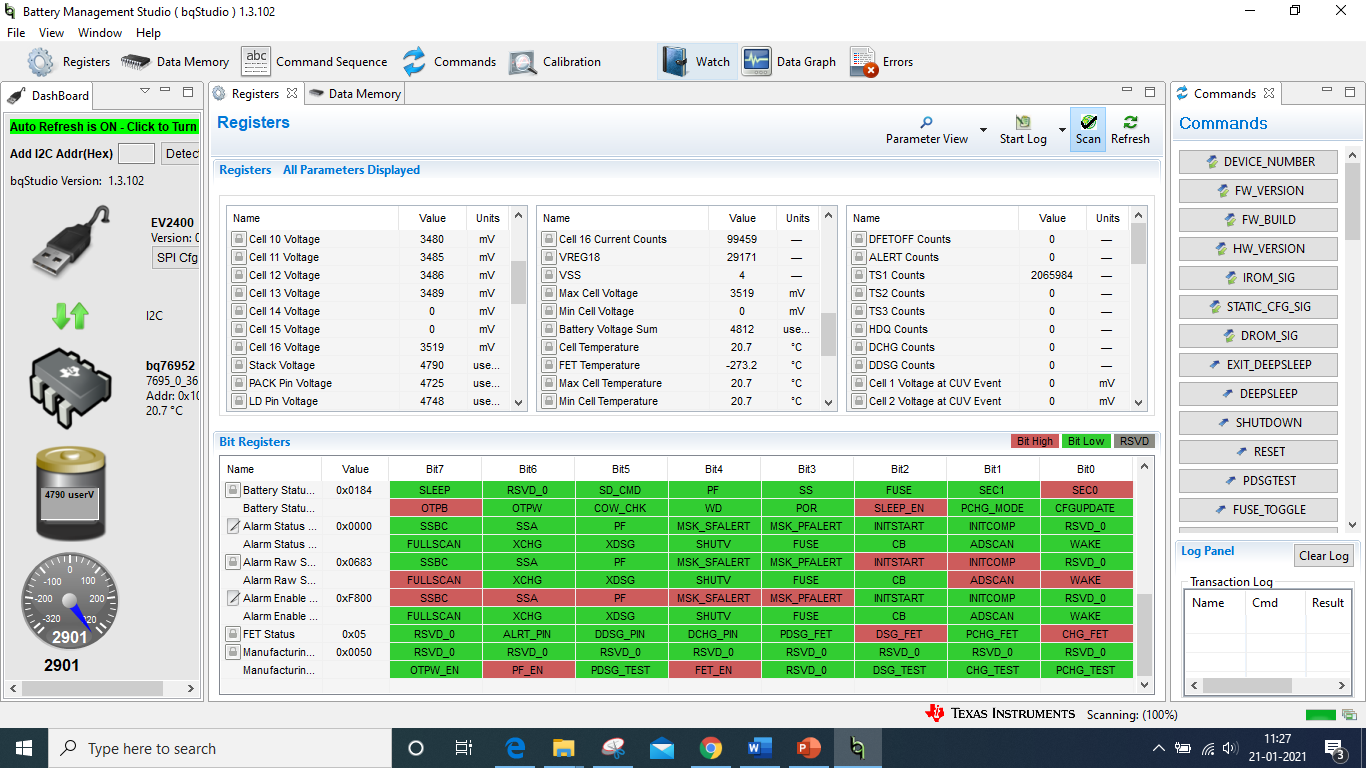
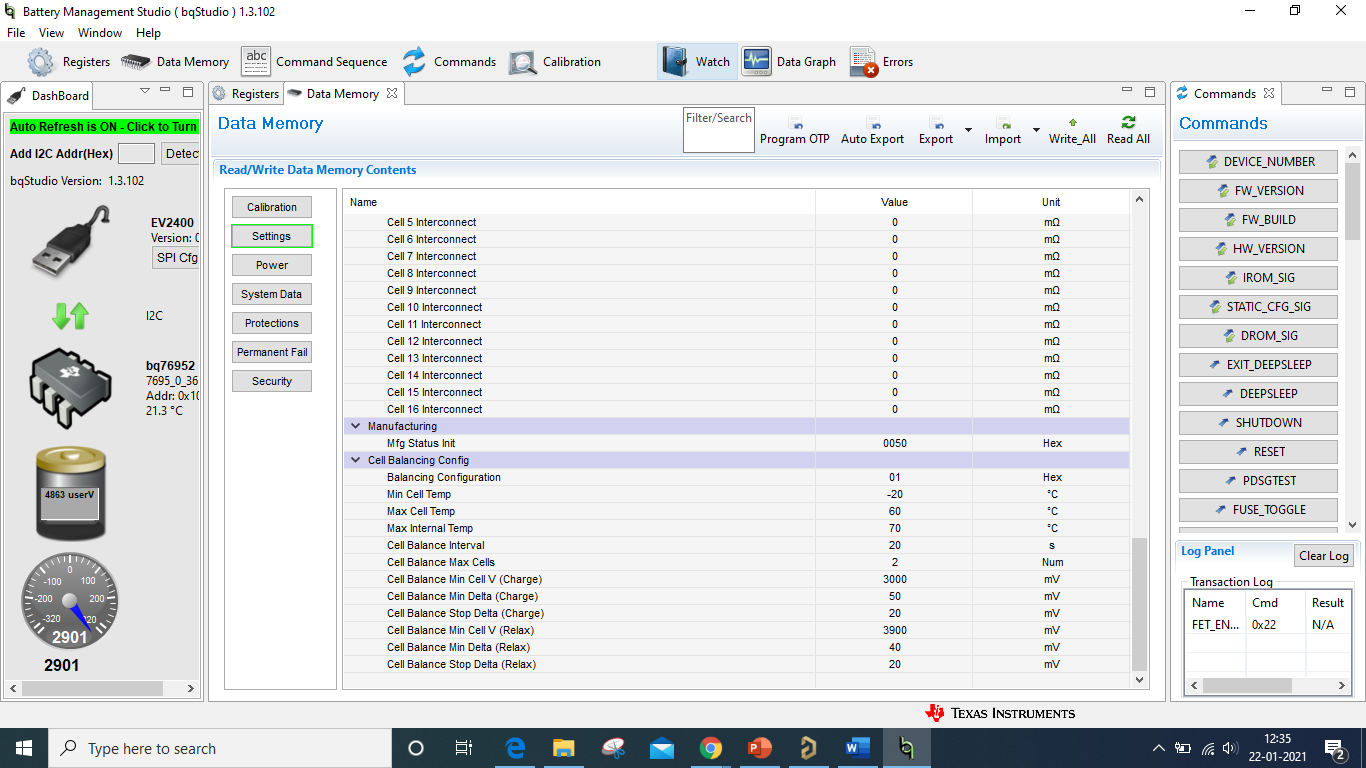
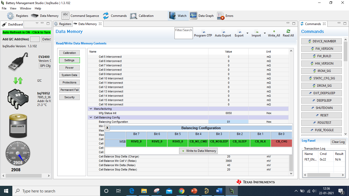
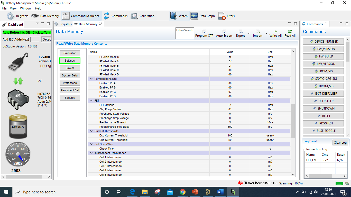
1. We are testing Battery pack14S2P with  BQ96952EVM(Seal Date-09/21/20), we set the cell balancing parameters during charging like  cell Balance Max cells, cell  balance min V/Delta etc  are shown in below image. 

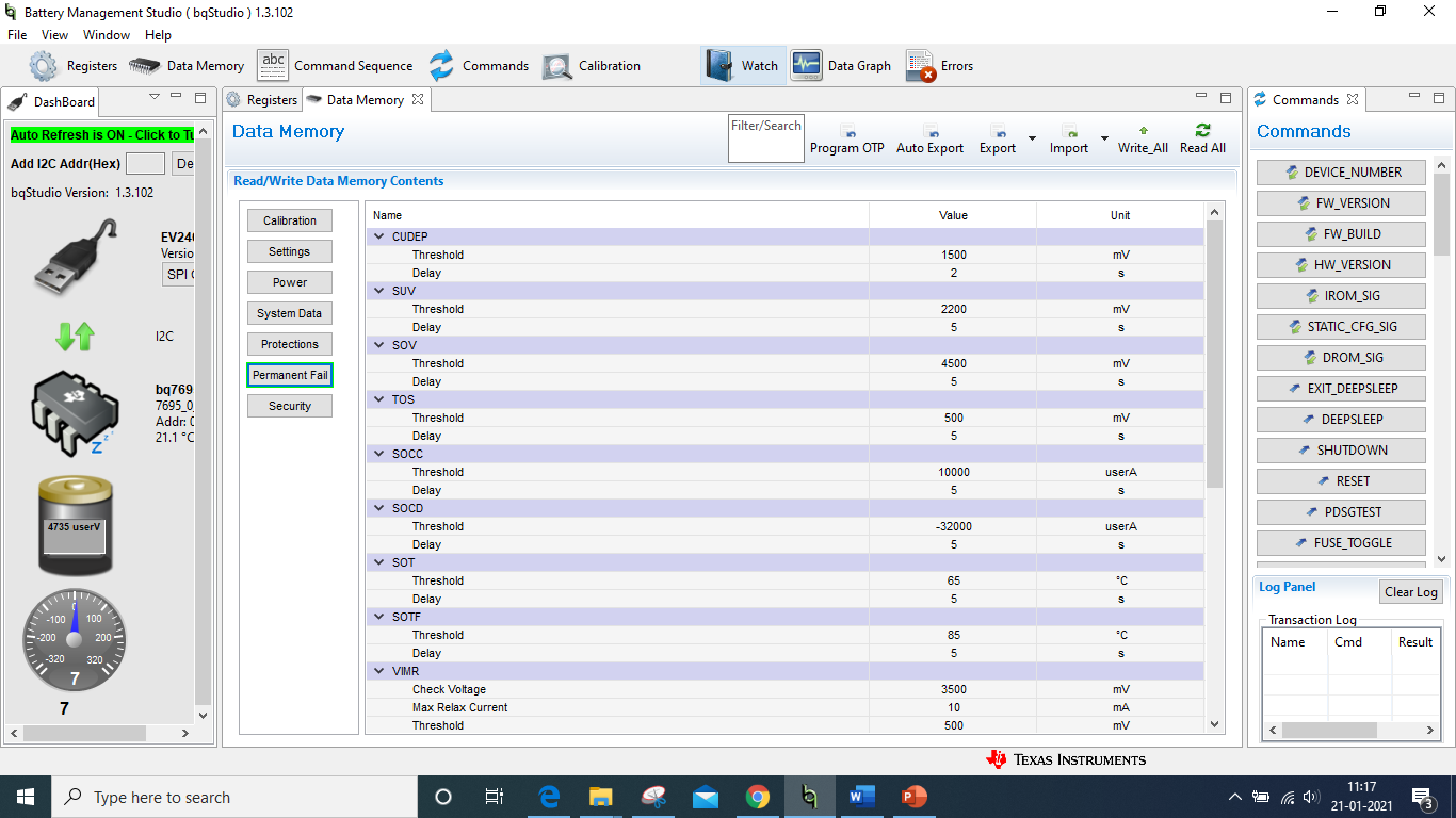
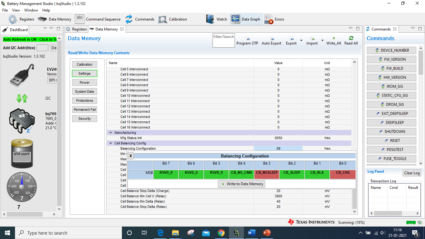
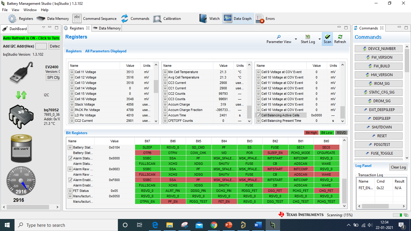
2.But during charging, Cell balancing is not observed, Cell balancing Active cells is always  0x0000  shown in below image,  and after some time FUSE(D3) LED is ON. So how can observe the cell balancing feature of this EVAL board 

3.How we can observe SOC feature of this chipset? 

4.In which condition, FUSE LED(D3) is ON, how can we off this LED(D3)?

  • Hi Shiv,

    The images in your message are not showing. Can you tell me what the top marking reads on the BQ76952 IC? Or you can also read the firmware version on the Dashboard of BQStudio to see which version of the device is on the EVM. If this EVM was ordered before the production version of the IC was released, the pre-production version of the device does not have the cell balancing feature. So it would be good to first confirm the device revision.

    The D3 LED on the EVM can be turned on by the BQ7718 secondary protectors or by the BQ76952 device (if configured for permanent failures to control the FUSE pin). The BQ771807 devices are set to turn on D3 if any of the cell voltages are greater than 4.45V. 

    This device is not a gauge, so it cannot report SOC. If you need an SOC feature, you need to include a battery gauge in your design like the BQ34Z100-G1. You can look at the TI Reference Design (TIDA-010030) as an example using this device. The BQ76952 does have an Accumulated Charge feature that can be very useful if you are trying to do gauging with your microcontroller.

    Best regards,

    Matt

  • Hello TI Team,

    Having good day!

    Thanks for your response

    1. As you asked some information are given below.

    Top marking on the BQ76952 IC is BQ76952 08WG4 A97Y.

    Device firmware version is 7695_0_36

    BQ software version is 1.3.102

    EVM Sealed Date(mention on EVM box)-09/21/20

    BQ software screenshot is shown below

    2. EVM board box screenshot is shown below

    3.What will we do if D3 LED is ON after some time if we configure setting in BQ software and start setup for cell balancing of 3 cell of 14S2P battery pack.

    4.Please mention proper settings and procedure  of  BQ studio software if we want to test (in autonomous mode) cell balancing of 3 cell of 14S2P battery pack.

  • It looks like you are using the final version of the device, so cell balancing should work. Can you export your .gg.csv file from BQStudio (click on Export on the Data Memory screen). I can check your settings to see why balancing is not working. 

    Do you have one of the cell voltages set higher than the others? If all cells are set to the same voltage, it will not try to balance.

    The D3 LED indicates that either the cell voltage is too high as detected by the BQ7718 secondary protectors or the BQ76952 is driving the FUSE pin high. You need to determine which is happening. Can you tell me the voltages for each of the cells?

    Thanks,

    Matt

  • Hello Matt Sunna,

    Having a good day!

    Thanks for reply to assist on time

    As per trailing mail you required some information & data, after that again we have done cell balancing testing with proper setup(14S2P battery pack) , now we are providing image of setting done  and data observed on BQ and voltages measured across cell and capacitors on  board,

    1. Voltage(V) across each cell  

    V1=3.038, v2=3.044, V3=3.459,V4=3.459, V5=3.457,V6=3.461,V7=3.459,V8=3.459,V9=3.455, V10=3.452,V11=3.457,V12=3.459,V13=3.460,V14=3.466

    2.Voltage(V) across capacitor filter of secondary protector IC(U2,U3,U4,U5)

    {C31=.061,C33=.006 ,C35=.038,}(We shorted two cell as our battery pack is 14S2P), C39=3.459

    C40=3.458, C43=3.455, C44=3.451, C46=3.454

    C48=3.457, C50=3.457, C51=3.459,C52=3.456

     C53=3.458,C55=3.458,C56=3.042,C57=3.037

    No higher cell voltage is found across any cell 

    3.Cell balancing set parameter

    4.Permenant failure(PF) setting resistor

    PF_EN

    PF_FUSE

    PF_2LVL


    6.Data memory screenshot

    7.CB resistor setting 

    7.At times,  if we only connect our battery pack(14S2P) to eval board, eval bord connect to BQ, No charging and discharging, After some time, D3 LED is ON

    8.Now D3 LED is not ON, After all setting , No we start charging On(500mA current), Now observed on dashboard , after some time D3 LED is On and No cell balancing is observed

    9. . Screenshot of dashboard after charging on is shown below

    8.EXPORT.gg.csb file(Save this file in our system)

    7206.EXPORT.gg.csv

    9.At time , we observed Red mark on any resistor value(showing in below screenshot) while changing any setting in data memory, what does it means, how to remove it.

    10.Please mention step(Setting of different resistor &set the threshold) in sequence order to do autonomous cell balancing during charging. How we observed on dashboard that cell balancing is doing its operation if it satisfying CB condition.

    11. Aprt from cell balancing issue, please answaer some of more queries,

    (i) what is the difference among OTD1, OTD2 & OTD3(we couldn't understand clearly by refering datasheet & technical manual , other information on TI website). What is the practical significance and why these three level protection tier is needed? can you provide more document on this topic that clearify more .

    (ii).What is difference between CC1, CC2 & CC3(we couldn't understand clearly by refering datasheet & technical manual , other information on TI website). what is the practical significance. Can you elaborate these concept that clearify more.

    (iii)What is the Relax mode?


    Please try to resolve this issue, as our project work is delayed due to finalization of this IC chipset


  • Hi Shiv,

    Thank you for sharing your data.

    From your screen captures, it looks like the FUSE bit is set in the BQ76952 status register which means the FUSE pin is detecting a high logic level. If this is on an EVM, then this must be coming from one of the BQ7718 secondary protectors. Can you determine which of the BQ7718 devices is driving its OUT pin high? Is this occurring during balancing. The cell voltages will change during balancing as the balance FETs turn on.

    The red color on the register field shows that the value has changed from the value previously read. (So red does not necessarily mean it is bad). If there is a problem writing to a register, there will be an error message at the bottom of the BQStudio window. 

    It looks like your cell balancing settings are correct as you showed in item #3. In the Register Window, you can observe the 'Cell Balancing Active Cells' parameter. I suggest you set the Parameter View to 'View Basic Parameters' to make it easier to observe.

    Regarding your other questions: 

    (i) what is the difference among OTD1, OTD2 & OTD3(we couldn't understand clearly by refering datasheet & technical manual , other information on TI website). What is the practical significance and why these three level protection tier is needed? can you provide more document on this topic that clearify more. I assume you mean OCD1, OCD2, OCD3. Many battery systems set multiple different over-current conditions - this is very common. For example OCD1 is set to a higher current threshold with a shorter delay and OCD2 is set to a lower threshold with a longer delay.

    (ii).What is difference between CC1, CC2 & CC3(we couldn't understand clearly by refering datasheet & technical manual , other information on TI website). what is the practical significance. Can you elaborate these concept that clearify more.

    This is described in the device datasheet. In general, you should use CC1 if you need an integrated current for battery gauging - it is updated every 250ms and measures the total integrated charge. CC2 is more useful for regular current measurements and is available every 3ms. CC3 is similar to CC2, but you can change the sampling rate to play with the speed/accuracy tradeoff.

    (iii)What is the Relax mode? This is basically Sleep mode. 'Relax mode' is a term often used with battery gauge devices.

    Best regards,

    Matt

  • Hello Matt Sunna,

    Thanks for reply,

    We resolved the issue of LED D3 ON. This is due to as we are using 14S2P battery pack, but we are not shorting Capacitor C31 & C33, and resistor R34 & R36(Secondary protector side) no mount. So after doing this  problem is removed.

    Cell balancing is observed by observing individual cell voltages, But we are still not unable to observe cell balancing on BQ deshboard.

    1.We set the parameters for cell balancing and configure some resistors are shown in below screenshot,

    2. In our battery pack, two battery cell voltage are lower than remaining 12 battery cell, Apply charging current(.50A, 56V) . But we observed that  during charging, cell1 & cell2 voltages are increasing continuously at a faster rate than rest of 12 battery cell, so observed cell balancing.

    But one doubt here, both cell1voltage  & cell2 voltage  is increased but datasheet saying it will balance alternatively, so here it is not like this

    On deshboard, Cell balancing active cell is not changing, cell balancing present time also not changing on BQ deshboard, so how we observed the cell balancing on dashboard. Status observed on deshboard is showing in below screenshot

    3. Is cell balancing active cell  configurable, how?

  • Hi Shiv,

    The Cell balancing active cell register will only show a non-zero value at the moment that balancing is taking place. I wonder if you may need to read this register more frequently to see this. Cell1 and Cell2 will both balance, but the device will alternate between the two. 

    Try using the logging feature of BQStudio. First, I recommend selecting Windows->Preferences->Show Advanced Views. This will change the view of the Registers screen and you should now see check boxes next to each parameter. I recommend selecting only the cell voltages and cell balance parameters. Then click Start Log. (On the Preferences menu, you can also change the Logging interval under Registers - I recommend changing it to 1000ms. It is set to 4000ms by default). 

    Regards,

    Matt

  • Hello Matt Sunna

    Thanks for reply