[FAQ] AM625 / AM623 / AM620-Q1 / AM62L / AM64x/ AM243x (ALV) / AM62Ax / AM62D-Q1 / AM62Px Design Recommendations / Commonly Observed Errors during Custom board hardware design –SD card Interface

Part Number: AM62L
Other Parts Discussed in Thread: AM62P, SYSCONFIG, AM62P5-Q1, AM625, SK-AM62A-LP, AM620-Q1, AM625-Q1, AM623, AM625SIP,

Tool/software:

Hi TI Experts,

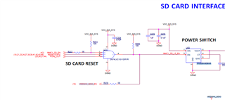
Is there a list of design recommendations or commonly observed errors for SD card Interface during Custom board hardware design?

Below are some common queries i have 

1. Pullup recommendations 

2. Power supply and Sequencing 

3. Series resistor for SD card clock output from the processor

4. Power switch for SD card reset 

  • Hi Board designers 

    Thank you for the interest.

    Please review the FAQ frequently for updates.

    Signal Description

    Signal Name Type Description
    SDCD Input SD Card / SDIO /e.MMC Card Detect
    SDCMD I/O SD Card / SDIO /e.MMC Command/Response Line
    SDWP Input SD Card Connector Write Protect Signal
    SDCK Output SD Card / SDIO /e.MMC Clock Signal
    SDDAT[3:0] I/O SD Card / SDIO /e.MMC data lines

    https://yannik520.github.io/sdio.html

    Peripheral Clock Output Series Resistor
    Series resistor on the clock output near to the processor clock output (MCSPI, MCASP) pins are recommended for possible reflection control (signal distortion) at the source of the clock output since the clock is also being used for retiming.
    For MMC0, MMC1, MMC2, OSPI0, GPMC0 interfaces, an unbonded pad is used (internal) for retiming. We do not use the same clock that is sent across the PCB to the attached device for our capture clock. We branch the output clock into two paths inside the device, where the clock is sent to two separate IO cells. One IO cell is connected to a package ball, which is used to source a clock to the attached device. The other IO cell is unbounded (not connected to any package ball). The clock we use as the receive capture clock is sent out through the unbounded IO cell and looped back into the device before being used as the capture clock. We do this so the clock has the same delay that is inserted on the clock going out to the attached device and the same delay that is inserted on the data coming back in from the attached device. The unbonded IO cell pad never experiences the voltage step that is produced on the source end of a PCB signal trace. A low value series resistor (0Ω to start) is recommended (provisioned) to control possible signal reflections (signal integrity purpose).

    Regards,

    Sreenivasa

  • Hi Board Designers, 

    Inputs regarding power supply

    Most CMOS semiconductor inputs are not fail-safe. So, there is a good chance the same requirement applies for the attached device. We expect the IO power rail of attached devices to be powered from the same power supply that is powering the associated AM64x IOs to prevent any sequencing issues. You will need to ensure your system implementation doesn't cause problems for either of the devices if they are not powered from the same source.

    I’ve just run into a weird thing in AM62P datasheet (SPRSP89A). In Table 5-1. Pin Attributes it states that MMC1_SDCD and MMC1_SDWP balls are powered by VDDSHV0. Is this true, or a datasheet bug?

    Other MMC1 pins are powered by VDDSHV5, and for other MMCs their power is not split this way (all MMC0 is from VDDS_MMC0, all MMC2 is from VDDSHV6).

    The MMC1_SDCD and MMC1_SDWP signal do not connect to the SD Card, so they do not need to be part of the VDDSHV5 power domain. These signals typically connect to a card detect switch and write protect switch in the SD Card connector. These signals need to be pulled up to the VDDSHV0 power rail and connected to the SD Card connector switches, which short the signals to VSS when a card in inserted or the write protect slider in the write protect position. The MMCSD1 host controller would lose the logic state of these signals when the VDDSHV5 power rail changed from 3.3V operation to 1.8V operation if they were powered from VDDSHV5, since the logic state inside the AM62Px device is not valid during a voltage change on the IO power rail. So, the power rial assignment of these signals was done this way on purpose to ensure the MMCSD1 host controller would not think the SD Card was removed when the VDDSHV5 power rail changes from 3.3V to 1.8V.

    (+) AM6442: VDDSHV5 and MMC1 - Processors forum - Processors - TI E2E support forums

    The VDDSHV5 power rail is being sourced from the internal SDIO_LDO, which has its input (VDDA_3P3_SDIO) connected to the same 3.3V power supply that is sourcing the SD Card and the SDIO_LDO output (CAP_VDDSHV_MMC1) is sourcing the VDDSHV5 power rail.

    (+) [FAQ] AM625 / AM623 / AM620-Q1 / AM625-Q1 / AM625SIP: Custom board hardware design - SD card (MMC1) VDD power supply - Processors forum - Processors - TI E2E support forums

    The 3.3V power switch controlled by the three input AND gate is needed to cycle power to the SD Card and the AM62x MMC1 IO power supply. The SD Card does not have a reset input, so cycling power is the only way to reset it. You must also cycle power to the AM62x MMC1 pins anytime you cycle power to the SD Card because the SD Card inputs are not fail-safe. Having the reset capability is very important for UHS-I SD Cards because this is the only way to force the SD Card back to 3.3V mode after it was changed to operate in 1.8V mode.

    I would not recommend a direct connection to 3.3V if you plan to support UHS-I SD Cards.

    (+) [FAQ] AM62A7 / AM62A3 / AM62A1-Q1 / AM62D-Q1: Why is MMC1 powered by two different voltage supplies, VDDSHV0 and VDDSHV5 ? - Processors forum - Processors - TI E2E support forums

    The logic state of the MMC1_SDCD and MMC1_SDWP inputs to the host must not change when a UHS-I SD Card changes its IO operating voltage. It is not possible to maintain a valid logic state if these signals propagate through an input buffer of a dual-voltage SDIO cell that changes voltage. So, these signal functions are assigned to IOs that do not change voltage. These signals only connect to switches in the SD Card connector, so there is no reason for them to change voltage when the SD Card signals change operating voltage. The MMC1_SDCD and MMC1_SDWP signals should be connected to the SD Card connector switches and pulled high with external pull resistors connected to VDDSHV0. The other MMC1 SD Card signals with pull-up resistors should have their pulls powered by the VDDSHV5 source that dynamically changes voltage. 

    The MMC2_SDCD and MMC2_SDWP pins are powered from the same power rail as the other MMC2 pins. However, you should not use these pins for the MMC2_SDCD and MMC2_SDWP signal functions if you are trying to connect an UHS-I SD Card to MMC2. For this use case, these signal functions would need to implemented using one of the other pin multiplexing options that uses an IO cell powered from a fixed voltage source. The MMC2 assignments are different because we only expected MMC2 to be used with on-board fixed voltage SDIO devices similar to WiFi or Bluetooth transceivers.

     (+) SK-AM62A-LP: pull down register for SD card clock - Processors forum - Processors - TI E2E support forums

    The AM62Ax IOs are turned off by default and will not be driving the SD Card signals until software has initialized the IOs. Therefore, external pulls are required for each of the SD Card signals to hold the SD Card input buffers in a valid logic state. Software should not be turning on any internal pulls for the IOs associated with SD Card since we require external pulls on each of the signals. Turning on the internal pulls could create a condition that violates the SD Card standard if the system designer uses external resistor values that result in a pull resistance less than 10k when combined with the internal pull resistor.

    Regards,

    Sreenivasa

  • Hi Board Designers, 

    Inputs regarding MMC1 interface 

    (+) AM625: Can MMC1 support 4bit eMMC - Processors forum - Processors - TI E2E support forums

    We only support SD Cards on MMC1 because it was not timing closed for eMMC devices.

    (+) AM2432: Pin connectivity Requirements for MMC1 - Processors forum - Processors - TI E2E support forums

    All of the pins associated with the MMC1 port default to an off state, so you do not need to do anything to them if not being used.

    See the highlighted portion of the following note, which can be found below the Pin Connectivity table.

    Internal pull resistors are weak and may not source enough current to maintain a valid logic level for some operating conditions. This can be the case when connected to components with leakage to the opposite logic level, or when external noise sources couple to signal traces attached to balls which are only pulled to a valid logic level by the internal resistor. Therefore, external pull resistors are recommended to hold a valid logic level on balls with external connections.

    Many of the device IOs are turned off by default and external pull resistors may be required to hold inputs of any attached device in a valid logic state until software initializes the respective IOs. The state of configurable device IOs are defined in the BALL STATE DURING RESET RX/TX/PULL and BALL STATE AFTER RESET RX/TX/PULL columns of the Pin Attributes table. Any IO with its input buffer (RX) turned off is allowed to float without damaging the device. However, any IO with its input buffer (RX) turned on shall never be allowed to float to any potential between VILSS and VIHSS. The input buffer can enter a high-current state which could damage the IO cell if allowed to float between these levels.

    (+) AM62A7-Q1: Regardin MMC1/MMC2 Port Connection with eMMC - Processors forum - Processors - TI E2E support forums

    It is not possible.

    The MMC1/MMC2 ports only have 4 data bits, and these ports were not timing closed to operate with eMMC devices.

    The MMC0 port is the only one that has 8 data bits and supports eMMC devices.

    Please refer to the MMCSD timing section in the datasheet to see what devices and data transfer modes are supported for each MMCSD port.

    As I discuss the eMMC suppler he told me.

    you can connect eMMC in 4-bit mode instead of 8-bit mode.

    You need to configure the eMMC driver in SoC to operate in 4-bit mode, H/W side - connect eMMC Data lines DAT0-DAT3 to SDIO lines, and other eMMC data lines (DAT4–DAT7) left unconnected in 4-bit mode

    Is there any way we can use eMMC as a SD card with4-bit mode.

    The issue is not related to bus width.

    The timing requirements defined in the eMMC standard have differences relative to the timing requirements defined in the SD Card standard. The MMC1/MMC2 ports were not timing closed to operate with the timing requirements defined in the eMMC standard. These ports were only timing closed to operate with the timing requirements defined in the SD Card standard.

    (+) LP-AM243: Regarding the MMC1 and μSD card usage - Arm-based microcontrollers forum - Arm-based microcontrollers - TI E2E support forums

    We have two IO implementations for MMC ports. One implementation is an actual eMMC/SDIO PHY that has dedicated signal functions for each pin and only supports 1.8V IO signaling. The MMC0 port on AM243x uses the eMMCPHY buffer type, which is an example of that implementation. The other implementation uses a slightly modified LVCMOS IO cell for each pin and they support multiplexing of other signal functions and 1.8V or 3.3V IO signaling. The MMC1 port on AM243x uses the SDIO buffer type, which is an example of that implementation.

    The buffer type implemented for each pin can be found in the Pin Attributes table and each buffer type has its own Electrical Characteristics section in the datasheet.

    (+) [FAQ] AM6422: SD Host controller driver strength - Processors forum - Processors - TI E2E support forums

    No. The drive strength of the SDIO buffer types associated with the MMC1 signals is fixed to 40 ohms.

    The IOs associated with the AM64x MMC1 port has nominal source impedance of 40 ohms. This should have been reflected in the AM64x IBIS model.

    The best way to determine optimum PCB traces impedance is to use the IBIS model from AM64x and the attached device in signal quality simulations. These simulations could be used to determine which specific PCB implementation provides adequate signal quality and signal rise/fall times (slew rate). I'm not an IBIS model expert, but fairly sure there is a model for each valid IO operating voltage. Let me know if that is not the case and I will assign this thread to our IBIS model expert.

    The IBIS model is the only way we define IO output characteristics.

    There are two options for changing the operating frequency of the MMC1 port. The MMCSD1 host controller has internal clock dividers that can be used to reduce the clock frequency of the MMC1 port, but these clock dividers may not provide much resolution in frequency changes. The other option would be to reduce the MMCSD1 function clock frequency, which may impact other subsystems that share the same clock domain inside the device. You may want to use the Clock Tree tool function in the SYSCONFIG tool to understand the internal clock structure of the AM64x device.

    (+) AM6442: Why only emmc0 can support emmc flash - Processors forum - Processors - TI E2E support forums

    Because the design team only closed timing of the MMC0 peripheral for operating with eMMC devices and only closed timing of the MMC1 peripheral for operating with SD Cards

    (+) TMDS243EVM: Is WR_PROTECT effective at 0 or 1? Is SD_DETECT effective with 0 or 1? - Arm-based microcontrollers forum - Arm-based microcontrollers - TI E2E support forums

    The "Standard Size SD Card Mechanical Addendum" recommends using an SD Card connector that has a card detection switch that is open when the SD Card is not inserted and closes when the SD Card is inserted. One side of the SD Card connector switch is connected to ground (VSS) and the other side of the switch is connected to the MMC1_SDCD signal which is pulled up to the respective IO supply via an external resistor. With this connection topology the MMC1_SDCD signal will be high when the card is not inserted and will be low when the card is inserted. 

    Note: VDDSHV0 is the IO supply for the AM243x MMC1_SDCD and MMC1_SDWP inputs, and VDDSHV5 is the IO supply for the other MMC1 signals. 

    The "Standard Size SD Card Mechanical Addendum" doesn't provide any specific recommendation for Write Protect.

    I do not think the MMCSD host controller has any specific logic state requirement for these inputs, and software can be configured to use an active-low or active-high signal for either of these signal functions. 

    (+) AM6421: Terminal for SD boot - Processors forum - Processors - TI E2E support forums

    From a hardware perspective, it is okay to power the MMC1 IO power rail (VDDSHV5) from a fixed 3.3V power supply when you do not plan to use UHS-I SD Cards, or you do not plan to use any of the faster 1.8V signaling data transfer modes supported by UHS-I SD Cards. You must ensure your software never tries to use any of the 1.8V signal modes if you ever attach an UHS-I SD Card. Therefore, your concern with what the ROM code does is valid.  For the proposed connection topology, you need to be sure the SD Card ROM boot code never uses any of the 1.8V signal modes if it detects a UHS-I SD Card.  I will let the ROM code team answer this question.

    VDDA_3P3_SDIO and CAP_VDDSHV_MMC1 should be connected directly to GND if the SDIO_LDO is not used to power VDDSHV5.

    The ROM code will use Legacy compatibility mode at low clock frequency 25MHz, and never attempt to increase frequency, regardless of the SD card capabilities.

    When using SDCD, is it possible to configure the power supply and signal level on the SDCD side to be only 1.8V?

    I'm not sure which MMC port you are asking about.

    The SDCD signal function associated with the MMC1 port is part of the VDDSHV0 IO power domain, so this signal must operate from the same power supply that is sourcing VDDSHV0.

    The SDCD signal function associated with the MMC2 port has three pin multiplexing options, where two are part of the VDDSHV0 power domain and the other is part of the VDDSHV6 power domain. The operating voltage of this signal must be from the same source being used to power the respective IO (VDDSHV0 or VDDSHV6 power domain).

    I do not understand why this is a concern. Normally the SDCD signal is only connected to switch on the SD Card slot, where the signal is pulled high with a pull-up connected to the same power rail that is powering the associated IO and the switch in the SD Card slot will pull the signal to VSS when a card is inserted. The switch doesn't care what voltage is applied to the pull-up.

    I understand about SDCD.
    When the VDDSHV5 is set to 1.8V using MMC1, the signals of DATA, CLK, and CMD are 1.8V, but is it possible to write to and read from the SD Card?

    SD cards begin operation at 3.3V. If using a UHS-I SD card, the software driver will request an IO voltage change to 1.8V for the higher speed modes. If you plan to support the higher speed modes of these cards, you will need to implement a dual voltage VDDSHV5 power supply that is able to change voltage at the same time the card is told to change voltage. Otherwise, you can power VDDSHV5 from a fixed 3.3V source if do not need to support the faster modes that require the signals to dynamically change from 3.3V to 1.8V. You should look at the TI EVM for an example of how to implement the SD card and VDDSHV5 power sources.

    I don't plan to use the UHS-I SD Card, so I'll consider using it with a 3.3V power supply.

    We still recommend implement a 3.3V load switch that sources the SD card and the MMC1 VDDSHV5 IO power rail with its enable controlled by a three input AND of the power on reset, AM62Ax warm reset output, and a GPIO that is pulled high until configured by software. This is needed to reset the SD card since it doesn't have a reset pin. The only way to reset an Sd card is cycle its power and the AM62Ax VDDSHV5 IO rail must be cycled at the same time to avoid non-fail-safe conditions. This implementation will reset the card anytime the system power is cycled, a warm reset is generated like in the case where a watchdog time resets the processor, or if the SD card software driver needs to reset it via a GPIO without resetting the entire system.

    The VDDSHV5 is always supplied, and the power supply of the SD card is loaded with a load switch.
    Is there a problem if the VDDSHV5 is always supplied to the SD card after SDCD is detected?
    Is it a substitute for a RESET if I put a load switch on the power supply to the SD card?

    Do I really need three inputs, SD_EN, RESETSTATz, and PORz_OUT, to power enable the SD card?
    Is it possible to achieve this with two signals, SD_EN and RESETSTATz?

    The IOs associated with both the AM62Ax device, and the SD Card are not fail-safe. This means no external circuit can source any potential greater than the potential applied to the respective IO power rail. See the "Steady-state max voltage at all other IO pins" parameter in the Absolute Maximum Ratings table in the datasheet, where the potential applied to a pin is limited to minimum of "-0.3V" and a maximum of "IO supply voltage + 0.3V".  The same limit should be applied to the SD Card pins.

    The IO power rails of attached devices need to always have the same potential applied to prevent current injection into an IO that has a potential applied greater than the limits defined in the datasheet. For example, if one device is turned on the other device must be turned on, if one device is turned off the other device must be turned off. Their IO supplies also need to track as the power source ramps up or down. The best way to ensure this condition, is to power the IOs associated with both devices from the same power source.

    For the SD Card use case, the VDDSHV5 power rail on AM62Ax, the SD Card, and any external pull-up resistors need to be powered by the load switch.

    For AM62Ax the MMC1 IOs default to an off state, so we recommend external pulls on the MMC1 signals to hold the inputs of the attached SD Card in valid logic state until the device has booted, and software configures the IOs. An external pull-down resistor is recommended for the CLK signal and external pull-up resistors are recommended for each of the CMD and DAT[3:0] signals. The external pull-up resistors should be powered from the same switched 3.3V power that is connected to the SD Card and the VDDSHV5 power rail.

    Our reset expert said the PORz_OUT would not be needed since the RESETSTATz output will satisfy all reset cases for the SD Card.

    I need to clarify my last reply. I should have said the RESETSTATz output will satisfy the power-on and warm reset functions for the SD Card. You will still need a two input AND gate to insert the software controlled GPIO reset function for the case where software needs to initiate a reset to only the SD Card.

    The software GPIO reset function originates form an IO expander on the TI hardware platform, but you could use a GPIO signal function associated with one of the AM62Ax pins if your system doesn't include the IO expander. Select an AM62Ax pin with a GPIO multiplexing option that is turned off by default. Connect a signal from this pin to the other input of the AND gate and include a pull-up on this signal so the SD Card is brought out of reset as soon as the RESETSTATz goes high. Software can configure the AM62X pin to operate as GPIO after boot and drive it low if it needs to reset the SD Card.

    (+) AM625: AM6252 Board + PMIC(TPS6521904) : SD Boot - Processors forum - Processors - TI E2E support forums

    Clarify how to boot from SD-card by AM62P EVM.

    If a system plans to support UHS-II SD Cards on MMC1, the VDDSHV5 IO supply and the SD Card must be power cycled any time the SD Card needs to be reset since it does not have a reset pin. Cycling power to the SD Card is the only way to return an SD Card back to 3.3V operation after it was previously operating at 1.8V. UHS-II SD Cards are required to begin communications with the host using 3.3V signaling so they are backwards compatible to the requirements of a legacy host. These cards can be changed to use 1.8V signaling to achieve faster data transfer speeds. The VDDSHV5 power rail must also be switched off when the SD Card power is switched off since the SD Card input are not fail-safe.

    There are two sections of circuits on the AM62P EVM schematic that accomplish the task of controlling power to the SD Card and VDDSHV5. The circuit that controls power to the SD Card can be seen on the schematic page titled "SD CARD INTERFACE".  The circuit that controls power to VDDSHV5 can be seen in a section titled "3.3V/1.8V SD CARD SUPPLY" on the schematic page titled "PERIPHERAL POWER SUPPLY -1". Both of these circuits are turned off any time reset is asserted or the GPIO connected to "MMC1_SD_EN" is driven low. This is required to force the SD Card and the VDDSHV5 power source back to 3.3V mode after a hardware or software resets, where it must reestablish communications with the host using 3.3V signaling.

    Note: the GPIO connected to "VSEL_SD_SOC" must default to a high logic state before reset is released to ensure the VDDSHV5 power supply is operating at 3.3V when SD Card communications is first initiated. This signal is only driven low at the same time the SD Card is told to switch from 3.3V to 1.8V and it shall never be allowed to go back to a logic high state until the SD Card is powered off or reset.

    Since reset is being used to turn the SD Card off, it is not possible for the SD Card to be powered up before reset is released.  The SD Card boot code in ROM is delayed for a period of time that should be long enough for the SD Card to power up and be ready for communications.


    Regards,

    Sreenivasa

  • Hi Board Designers,

    Refer below  for information related to SD card reset.

    AM62P5-Q1: RESETSTAT and PORz_OUT for SD card power enable

    In the schematic of AM62P EVM, RESETSTATz and PORz_OUT are ANDed to the SD Card power enable signal.

    Customer also understand that RESETSTATz is also asserted when PORz_OUT is asserted.

    Is this understandig correct ?

    Is the circuit like this because the timing is slightly different when asserting?

    In that case, please tell us what  the timing between RESETSTATz and PORz_OUT.

    The system power on reset is connected to ensure the card power is forced off as soon as power is applied since this reset is expected to be valid while power supplies ramp.  The RESETSTATz is included so the SD Card is power cycled (Reset) if there is a processor warm reset source like a watchdog time-out. The GPIO is connected to allow the software driver to reset (cycle power) the SD Card.

    The RESETSTATz will not be valid until all AM62Px power rails are valid, so it is delayed relative to the system power on reset.

    Regards,

    Sreenivasa

  • Hi Board designers, 

    Please Refer below for inputs related to supported standards.

    (+) AM6411: What's the right Spec. for SDIO? - Processors forum - Processors - TI E2E support forums

    https://e2e.ti.com/support/processors-group/processors/f/processors-forum/1548389/am6411-what-s-the-right-spec-for-sdio

    please refer the data sheet.

    6.10.5.12.2 MMC1 - SD/SDIO Interface

    6.10.5.12.2 MMC1 - SD/SDIO InterfaceMMC1 interface is compliant with the SD Host Controller Standard Specification 4.10 and SD Physical Layer Specification v3.01 as well as SDIO Specification v3.00 and it supports the following SD Card applications:

    • Default speed

    • High speed

    • UHS–I SDR12

    • UHS–I SDR25

    • UHS–I SDR50

    • UHS–I SDR104

    • UHS–I DDR50

    We verified the TRM content internally.

    The datasheet is correct and references to 4.x in the TRM will be updated.

    Expert comments:

    I wanted to understand what got defined in 4.0 relative to 3.0.  It looks like embedded SDIO was added to 3.0, which is what we support.  It looks like UHS-II was added to 4.0, which we do not support.  So, revision 3.0 is definitely correct.

    Regards,

    Sreenivasa

  • HI Board Designers, 

    (+) AM62L: MMC - Processors forum - Processors - TI E2E support forums

    Inputs related to supported standards

    Do all three MMC/SD buses support eMMC 5.1, SD 3.0, and SDIO Version 3.0?

    2、What does the content shown in the following picture mentioned in the TRM manual mean? Does it support SD 4.10 and SDIO 4.0? So, should we follow the data manual or the TRM?

    The next revision of the AM62Lx datasheet will be updated to show with the following list of devices and data transfer modes supported for each MMC instance.

    The MMC0 port supports connections to an eMMC device or embedded SDIO device. It does not support removable SD Cards.

    The MMC1 and MMC2 ports support connection to a removable SD Cards or embedded SDIO device. They do not support eMMC devices.

    What does the content shown in the following picture mentioned in the TRM manual mean? Does it support SD 4.10 and SDIO 4.0? So, should we follow the data manual or the TRM?

    For the SDIO specifications, please follow the data sheet.

    The references to 4.x in the TRM will be updated.

    egarding the MMC interface of AM62Lx, does MMC0 support a 1-bit wide data bus or a 4-bit wide data bus? And do MMC1 and MMC2 support a 1-bit wide data bus?

    Is this a generic query or do you have an use case for the query.

    As a general answer, MMC0 should be able to support 4-bit or 1-bit and MMC1/MMC2 should be able to support 1-bit.

    I ever have similar support needs to support 2 eMMC, even one can be 4bit mode. which was supported on AM335x, but new AM62x can only support one, is it just not verified/tested? or the IP can't support 4-bit eMMC on MMC1?

    eMMC is only supported on MMC0. We did not close timing of any other MMC port to be compliant to the eMMC timing requirements.

    Regards,

    Sreenivasa

  • Hi Board Designers,

    Inputs related pulldown for Clock and SDCD 

    https://e2e.ti.com/support/processors-group/processors/f/processors-forum/1531431/am62p-stalls-and-crashes-during-boot-and-runtime?tisearch=e2e-sitesearch&keymatch=r0p4#

    We found that the stalls and crashes during boot and runtime were linked to the SD_CD# signal. We use the internal pull-up on that signal, but due to this https://lore.kernel.org/all/20250221091447.595199-1-mwalle@kernel.org/, the configuration was reset when the GPIO was requested, causing the SD_CD# signal to float. This probably caused some noise at lower temperatures causing an interrupt storm. We were able to reproduce this at room temperature by applying a PWM signal to the SD_CD# line.

    We would still like to know what issues could be triggered by not having the MMC1_CLK pull-down, and whether it would also be safe to not assemble it so that we would not need to redesign our board.

    In my understanding, it prevents the signal from floating before it is driven by software. We drive that signal in U-Boot and Linux, so is that MMC1_CLK pull-down necessary?

    The AM62Px IOs associated with the MMC1 signals are turned off until software boots and initializes the MMCSD1 host controller and the PADCONFIG registers associated with each MMC1 signal function. Without the external pull-down, the SD Card clock input will be floating until software has completed the initialization of the MMC1 peripheral.

    Allowing a CMOS input buffer to float is not a good design practice. Allowing this to happen can compromise long-term reliability of a device due to excess shoot-through current on any input buffer connected to a floating signal.

    A floating clock signal could also allow the SD Card to receive short duration glitches on its internal state machine clock. These short duration glitches are likely to over-clock the logic circuits in the SD Card state machine, which could cause it to enter an unexpected or locked state. SD Cards do not have a reset input. The only way to reset the SD Card is to cycle its power, which means you also need to cycle the power supply that sources the VDDSHV5 IO power rail. 

    Note the recommendation for adding a 100R series resistor for the SDCD pin.

    Regards,

    Sreenivasa

  • (36) [FAQ] AM625: What's the purpose for the pull down R on MMC_CLK? - Processors forum - Processors - TI E2E support forums

    [FAQ] AM625: What's the purpose for the pull down R on MMC_CLK?

    Most of the IOs associated with the AM62x device default to the off state, which means any attached device input without an internal pull resistor would be floating until software configures the pin to drive the signal. We use an external pull-down rather than an external pull-up since the clock signal is held in a low logic state when paused.

    Pull down vs pull up for SD card clock

    Because there are cases where the clock is stopped or paused in a low logic state and the pull-down option is consistent with this logic state.

    SK-AM62A-LP: pull down register for SD card clock

    Clock line of SD card is pull down on EVM. Can you please let us know the reason? Padconfig setting is also internal pull down in SDK.

    The AM62Ax IOs are turned off by default and will not be driving the SD Card signals until software has initialized the IOs. Therefore, external pulls are required for each of the SD Card signals to hold the SD Card input buffers in a valid logic state. Software should not be turning on any internal pulls for the IOs associated with SD Card since we require external pulls on each of the signals. Turning on the internal pulls could create a condition that violates the SD Card standard if the system designer uses external resistor values that result in a pull resistance less than 10k when combined with the internal pull resistor.

    Because it is pulled down by R315 on another page of the schematic.

    You should never have a pull-up and pull-down connected to a digital signal at the same time since this would result in a mid-supply steady-state condition, which is not allowed on most CMOS inputs

    Regards,

    Sreenivasa

  • Hi Board Designers,

    Inputs related to SD card pullups

    (+) [FAQ] AM620-Q1: What's the max current input (or output) for SDIO DATA/CMD line? - Processors forum - Processors - TI E2E support forums

    AM620-Q1: What's the max current input (or output) for SDIO DATA/CMD line?

    We define output current as IOL and IOH parameters, which is the minimum Low Level Output Current and High Level Output Current for which the device is able to maintain the specified VOL and VOH values. Values defined by these parameters should be considered the maximum current available to a system implementation which needs to maintain the specified VOL and VOH values for attached components.  You will need to use the AM62x IBIS models in a simulation to determine VOL or VOH levels for a specific current.

    We plan to include the following input leakage note in the next revision of the datasheet.  Hopefully, it helps explain what this parameter defines.

    This parameter defines leakage current when the terminal is operating as an input, undriven output, or both input and undriven output,
    without internal pulls enabled.

    Most of the AM62x pins will be turned off after power-up. This means the input buffer is disabled, the output buffer is disabled, and the internal pulls are disabled.  Please reference the Pin Attributes table in the datasheet to see the initial power-up state of each pin. You may need to have external pull resistors on any signals that connect to inputs of attached devices to prevent them from floating until software configures the associated IO cell.

    You can use the AM62x internal pull resistors if an external resistor is not required to hold inputs to a valid state while waiting for software to configure the internal resistors. 

    The max input leakage is defined for the two worst-case conditions, which occurs when the voltage applied to the input is 0V or the IO power rail potential. See the test conditions associated with the input leakage current parameter. We do not define input leakage at VIL or VIH, but the leakage current will decrease as the voltage potential applied to the input moves away from either of the two test conditions.

    Recommended pullup for SD card interface 

    Is there a reason for 47K vs 10K

    Use of 47K ensures the SD card interface is within the SD card specifications in use cases where the SOC internal pulls are enabled unexpectedly.

    You should have an SD Card receptacle connected to MMC1 and the MMC1_SDCD signal should be pulled high by the same source that is sourcing VDDSHV0. The switch in the SD Card receptacle should be the configured such that it connects the MMC1_SDCD signal to VSS when a card is inserted. The high to low transition on the MMC1_SDCD signal will tell the host controller a card has been inserted.

    Regards,

    Sreenivasa

  • Hi Board Designers,

    Inputs related to supported interfaces on MMC0 and MMC1

    You should be looking at the MMC0 - eMMC Interface section in the Timing and Switching Characteristics section of the datasheet.  This is where the datasheet defines valid modes of operation.

    (+) AM6442: Why only emmc0 can support emmc flash - Processors forum - Processors - TI E2E support forums

    Because the design team only closed timing of the MMC0 peripheral for operating with eMMC devices and only closed timing of the MMC1 peripheral for operating with SD Cards.

    AM64x does not support SD Card on MMC0. More details provided below.

    It was not possible to close timing on the MMC0/MMC1 ports for them to be compliant with both eMMC and SD Card standards, so MMC0 timing was optimized for eMMC and MMC1 timing was optimized for SD Card.  You may find MMC0 timing is compliant to timing requirements of some SDIO devices, but you would need to perform a detailed timing analysis using system specific PCB delays, switching characteristics, and timing requirements of each device to confirm

    The external pull requirements vary based on the PHY implemented for a specific host port and the attached device. The PHY implemented for the AM64x MMC0 port only supports eMMC devices and does not require external pulls to hold the attached device in a known state until the port is initialized because the MMC0_CLK pin is driven internal pulls are automatically turned on as soon as the AM64x device is powered. That is not the case for MMC1.  

    (+) AM6442: Does MMC1 controller support Wifi SDIO devices ? - Processors forum - Processors - TI E2E support forums

    There should not be any issue connecting an SDIO device to MMC1 from the hardware perspective as long as you do not violate the timing conditions and timing requirements defined in the datasheet for the respective mode of operation.

    The MMC1 - SD/SDIO section of the AM64x datasheet says "MMC1 interface is compliant with the SD Host Controller Standard Specification 4.10 and SD Physical Layer Specification v3.01 as well as SDIO Specification v3.00 and it supports the following SD Card applications:" then provides a list of supported data transfer modes.

    Regards,

    Sreenivasa

  • Hi Board Designers,

    Inputs related to UHS-I SD card interface: Resetting SD card supply and processor IO supply

    I am using power switch to reset the SD card. When the SD card is reset the SOC IO supply is present. 

    Is there a performance concern with this configuration

    The processor MMC1 (VDDSHV5) or MMC2 (VDDSHV6)  power rail and the external pull-ups is required to be powered from the output of the SDIO_LDO. 

    The SD Card pins are not fail-safe so the input of SDIO_LDO needs to be power from the same switched power source used to power the SD Cards. 

    This will cycle power to the IOs and the external pull-ups at the same time so they are not sourcing any potential to the SD Card pins when it doesn’t have power.


    Having a potential on the SD Card pins when not powered may hold the SD Card power rail above the maximum voltage allowed to ensure a valid reset on power up or power-cycle.


    https://www.vikingtechnology.com/wp-content/uploads/2021/03/SDCard_Phison_PS8210_Industrial.pdf

    Regards,

    Sreenivasa

  • Hi Board Designers,

    FYI regarding output parameters

    (+) AM6411: MMC/SDIO drivers rise/fall timing and slew rates - Processors forum - Processors - TI E2E support forums

    Could you provide the rise/fall times and slew rates of drivers (IO cells) of MMC1 (SDIO) at 3V3 and 1V8 in different modes (specially default mode at <25MHz)?

    We do not define output rise/fall times because these parameters depend on the actual system implementation. You will need to use the IBIS model for the respective AM64x pin and simulate the rise/fall times based on your actual PCB load.

    Regards,

    Sreenivasa

  • Hi Board Designers,

    Inputs related to connection of internal LDO

    (7) AM6442: VDDSHV5 and MMC1 - Processors forum - Processors - TI E2E support forums

    The VDDSHV5 power rail is being sourced from the internal SDIO_LDO, which has its input (VDDA_3P3_SDIO) connected to the same 3.3V power supply that is sourcing the SD Card and the SDIO_LDO output (CAP_VDDSHV_MMC1) is sourcing the VDDSHV5 power rail.

    Regards,

    Sreenivasa

  • Hi Board Designers,

    Inputs related to SD card pulls

    (+) AM625: Sysconfig issue about AM6254 - Processors forum - Processors - TI E2E support forums

    How did we design this pull-up resistance state?

    SD cards were designed with the expectation they would be connected to a host that is always driving or pulling the signals to a valid logic state. However, that is not the case for AM62x because the pins associated with these signals have multiple signal functions. The IOs for these pins are turned off by default since the pins are not dedicated to the SD Card signal functions. This is done to prevent any contention with the actual use case. For example, there is a very good chance you would not want the pin associated with CLK to be driven if you were using it with the GPIO signal function. The internal pulls are also turned off for the same reason, as they may conflict with the actual use case.

    The SD Card inputs can't be left floating until software boots and configures the AM62x IOs, so external pulls are required to hold the SD Card inputs in a known state. There is no reason for software to turn on the internal resistors if an external resistor is already connected.

    We typically recommend an external 47k pull-up on CMD and each DAT signal, and an external 10K pull-down on CLK.

    Regards,

    Sreenivasa

  • Hi Board Designers,

    Inputs related to boot delay when SD card interface is used:

    (+) AM62A7: The boot time slows down by about 1 second when no SD card is inserted. - Processors forum - Processors - TI E2E support forums

    (+) AM62P: sdhci-am654 fa00000.mmc: Power on failed - Processors forum - Processors - TI E2E support forums

    The 1.5 seconds delay is coming because of the following commit:

    https://git.ti.com/cgit/ti-linux-kernel/ti-linux-kernel/commit/?id=7ca0f166f5b2

    As explained in the commit message, it may not be possible to remove the delay as long as the SDHCI1 node is enabled in the DTS.

    Regards,

    Sreenivasa

  • Hi Board Designers,

    Inputs related to PMIC TPS6593 configured for SD card functionality supporting uHS-I SD card

    (2) TPS6593-Q1: LDO1 output for SD card interface - Power management forum - Power management - TI E2E support forums

    AM62Ax SD card interface using TPS6593 PMIC

    SOC

    PMIC

    https://www.ti.com/lit/ug/slvucm3/slvucm3.pdf

    3.2 Control Mapping

    GPIO9 and GPIO11 are configured to enable LDO2 (VPP) and LDO1 (SD card interface). The TPS65931211-Q1 enables LDO1 when a rising edge is detected on GPIO11 after nRSTOUT is released and PMIC is in Active state. Similarly, the PMIC enables LDO2 when a rising edge is detected on GPO9 after nRSTOUT is released.

    GPIO5, GPIO6 and GPIO10 are configured to set the output voltages on some of the PMIC power resources and the state (high or low) for these GPIOs need to be set before the assigned rail turns ON. GPIO5 is configured to set the output voltage on LDO1 to support UHS-I SD cards (3.3V or 1.8V). GPIO6 is configured to set the voltage on the multiphase Buck1/2/3 to support either VDD_CORE voltage (0.75V or 0.85V). GPIO10 is configured to set the voltage on Buck4 to support LPDDR4 (1.1V) or DDR4 (1.2V).

    Note: In case SD card power control switch that switches the SD card power and also provides Low-High transition for PMIC is not implemented, LDO1 output will be disabled.

    Regards,

    Sreenivasa

  • Hi Board Designers,

    Inputs related to the clock transition

    (+) AM625: SDIO_CLK quality check - Processors forum - Processors - TI E2E support forums

    On customer board, connect MMC2 with WIFI module via serial inductance to eliminate overshot, probe on inductance of AM62 side, the clock signal has some reflection on edge, on WIFI side, the rising/falling edge is clean, we think on WIFI side should be OK, will the AM62 side clock quality impact AM62 SDIO receiving data?

    In other word, as the SDIO_CLK is a output signal, will AM62 MMC use the external clock for receiving?

    The AM62x MMC2_CLK pin is an output only. We implement another IO on the device, which is not connect to package balls. This undocumented IO is used to loop back the clock for retiming purposes. Therefore, you do not need to worry with non-monotonic transitions on the AM62x end of the signal trace.

    So same for MMC0_CLK and MMC1_CLK?

    Yes.

    Regards,

    Sreenivasa

  • Hi Board Designers,

    Inputs related to UHS-I receive mode training 

    (+) [FAQ] AM625 / AM623 / AM620-Q1 / AM625-Q1 / AM625SIP: UHS-I SDR104 Receive mode timing - Processors forum - Processors - TI E2E support forums

    [FAQ] AM625 / AM623 / AM620-Q1 / AM625-Q1 / AM625SIP: UHS-I SDR104 Receive mode timing

    Datasheet section 7.11.5.16.2.7 only provides Transmit Mode timings.
    My customer is asking for receive mode timings.

    The AM62x device only supports data training for UHS-I SDR104, which means the setup and hold requirements associated with the AM62x input data path are not fixed values that can be defined in the datasheet.

    (+) AM625: MMC1/MMC2 USH-I SDR50 SDR104 receive mode timing requirements - Processors forum - Processors - TI E2E support forums

    These data transfer modes require data training to center data capture in the center of the data valid window, so the timing requirements are not fixed to specific values.

    This is defined in the "MMC1/MMC2 DLL Delay Mapping for all Timing Modes" table.

    (+) AM625: HW Design to Support SD UHS-I Mode - Processors forum - Processors - TI E2E support forums

    (+) AM6422: spread spectrum clocking: restrictions when using UHS-I SD Cards - Processors forum - Processors - TI E2E support forums

    (+) AM6411: What's the right Spec. for SDIO? - Processors forum - Processors - TI E2E support forums

    Regards,

    Sreenivasa

  • Hi Board Designers, 

    FYI.

    The configuration of MMCSD2 was not quite clear. In the datasheet and dev-data.c, we could only find the description of MMCSD0/1.

    Do we have related documents for customer to debug MMCSD2? 

    (+) AM62x: MMCSD2 Configuration - Processors forum - Processors - TI E2E support forums

    MMCSD2 is basically another instance of MMCSD1 with respect to it supporting SD Card and SDIO devices operating in one of the data transfer modes listed in the datasheet.

    Regards,

    Sreenivasa

  • Hi Board Designers, 

    Inputs related to recommended pulldown value for the attached memory device pulldown:

    Memory interface peripherals pulldown value AM62x or Am64x 

    I have a few customer using 1K pulldown for some of the signals from the SOC mostly for memory interfaces.

    Wanted to get your thoughts on the use case.

    The current draw from the IO seems more and could affect the VOH. Any thoughts on the use case please.

    I agree the 1k resistor could impact the VOH level to the attached device, and it could also impact our VIHSS level if our receiver is turned on. 


    The customer should run a simulation of their system using the IBIS models of each device connected to the signal to determine if the output can achieve an appropriate levels after accounting for the output buffer drive capability, worst case pull resistance, and worst case leakage of all attached components.  I would suggest they consider a 4.7k if there is a concern with 10k.

    information on sizing of external pulls.

    A resistor must be selected that is able to hold the signal above the steady-state high (VIHSS) or below the steady-state low (VILSS) based on the signals worst-case combination of leakage, which will be the sum of the max leakage of all attached devices. 

    For example, if it is assumed AM62P is connected to a single UART device that has a max leakage of 5uA when operating at 1.8V.  The worst-case leakage would be 10uA + 5uA = 15uA.  VIHSS for the LVCMOS IO cell operating at 1.8V is 0.85 x VDD = 1.53V.  A pull-up resistor value would need to be at less than 18k ohms to hold the voltage above 1.53V for a worst-case leakage of 15uA.  It is suggested to use a value that is less than 18K ohm for this example.

    Regards,

    Sreenivasa

  • Hi Board Designers, 

    AM644x, AM243x, AM62L VDDA_3P3_SDIO (internal LDO input connection)

    The VDDA_3P3_SDIO connects to the SD card power switch output.

    I assume VDDA_3P3_SDIO is treated as a supply rail and the slew rate requirements for the other supply rails is applicable for the VDDA_3P3_SDIO supply input.

    Any thoughts please.

    Yes.  The ramp limit is associated with the ESD circuit implemented on each power rail, so the same limit applies to all power rails.

    Additional inputs on SOC IO ESD protection

    The IOs associated with the AM62Px device are not fail-safe. This means no external circuit can source any potential greater than the potential applied to the respective IO power rail. See the "Steady-state max voltage at all other IO pins" parameter in the Absolute Maximum Ratings table in the datasheet, where the potential applied to a pin is limited to minimum of "-0.3V" and a maximum of "IO supply voltage + 0.3V".

    The IO power rails of attached devices need to always have the same potential applied to prevent current injection into an IO that has a potential applied greater than the limits defined in the datasheet. For example, if one device is turned on the other device must be turned on, if one device is turned off the other device must be turned off. Their IO supplies also need to track as the power source ramps up or down. The best way to ensure this condition, is to power the IOs associated with both devices from the same power source.

    The ESD protection circuits associated with an IO will turn on if the potential applied is greater than IO supply voltage+0.3V.  This condition will inject current from the external voltage source through the ESD circuits to the IO power rail. We do not allow injection current through the ESD protection circuits because they were only designed to protect the device from short-duration ESD events similar to what would be introduced by a Human Body Model to account for device handling and a Charged Device Model to account for PCB assembly equipment. The ESD protection circuits are not designed for steady-state DC current. They also were not designed to provide any system-level ESD protection once the device has been installed on a PCB.

    Regards,

    Sreenivasa