Hi Team,
Would you please teach the memory map address for MPU_RAMとMPU_L2?
Thanks and Best regards,
Kuerbis
This thread has been locked.
If you have a related question, please click the "Ask a related question" button in the top right corner. The newly created question will be automatically linked to this question.
Hi,
As mentioned in SOC TRM section 1.3.1:
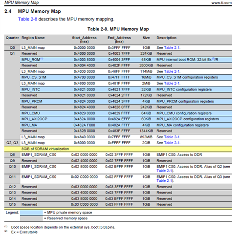
Please go through SOC TRM - chapter 2 - for more details.
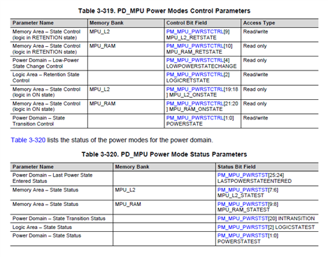
note about naming convention followed in TRM:-
if any thing is core specific other than MPU, it will be prefix by core name like DSP_, IPU_, etc. If any core specific prefixes are not there you can assume it for MAIN domain.
Hi Akash,
Thank you for replying.
I couldn’t find MPU_RAM and MPU_L2 in the Table 2-8. MPU Memory Map.
The customer wants to know MPU_RAM and MPU_L2 address which is describe in the Table 3-319&20 for power consumption.
Thanks and Best regards,
Kuerbis
Kuerbis,
Those memories function as cache and are not directly addressable (i.e., not memory mapped SRAM).
Regards,
Kyle
Hi Kyle,
MPU_L2 is MPU_L2 CACHE (1MB). Right?
Where is MPU_RAM? Is it L1 caches?
The customer would like to know it to understand PM_MPU_PWRSTCTRL register for power consumption.
Thanks and Best regards,
Kuerbis
Hi Kyle,
Do you have any update for this questions?
The customer is waiting for an answer.
Thanks and Best regards,
Kuerbis
Kuerbis,
MPU_RAM corresponds to the L1 Caches and RAM and MPU_L2 corresponds to the L2 Caches and RAM.
Regards,
Kyle
Hi Kyle,
Thanks!
Thanks and Best regards,
Kuerbis,